NVIDIA Kepler speculation thread

It depends how you count under what circumstances. SRAM probably shrinks close to theoretical scaling, most logic won't. Do you remember the discussion about gate first vs. gate last and GF claiming about 10% higher density than TSMC?
You only get the 1.95 scaling (TSMC indeed gives this number) when you compare 40nm and 28nm with a special set of layout rules. In my opinion, that number is a bit made up and not that relevant for a lot of cases. TSMC also gives the scaling without those rules (i.e. a more conventional layout without putting redundant structures in to get it as regular as possible) and then the claimed density scaling reduces to a mere 1.6. As an average (logic and SRAM mixed on a chip and the layout pays at least some attention to the 28nm layout peculiarities), I think a ~1.8 scaling is somewhat realistic (which also matches the claim of 10% better scaling with GF's 28nm HKMG processes).

There goes my buffer of not doubling ROPs and memory interface. :) Seriously though, even with 1.8x you could stuff as much as 3.5 billion transistors into GF104/b's die size for a 28nm part which should be more than enough for the above.
 
Actually (Ailuros hinted already to that direction above), nVidia said in some presentations that they will use (V)LIW3 for the Einstein architecture, which is the base for Echelon. For single precision it looks like two vec2 ALUs with 1 L/S, for DP it's just two DP ALUs + L/S.

Oops. :oops:

Still, that's… puzzling.
 
Isn't (V)LIW a reasonable way to increase single thread performance without blowing your power budget? On problems where you don't have hundreds of thousands of things to crunch on, this seems important.
 
Instruction bundling in long words is primary a way to pack maximum raw computing performance, by relying on compiler flexibility to exploit maximum utilization. This comes at expense of using very simple (static) scheduling, that otherwise would take away from both power, area and transistor budget. This is especially valid for parallel architectures, like GPU. Intel's Itanium is one rather exotic exception of this general approach.
 
There goes my buffer of not doubling ROPs and memory interface. :) Seriously though, even with 1.8x you could stuff as much as 3.5 billion transistors into GF104/b's die size for a 28nm part which should be more than enough for the above.
If you take Tahiti as an example, you can pack 4.3 billion transistors in that dies size. With a 256bit memory interface probably even more like 4.5 billions. :LOL:
Instruction bundling in long words is primary a way to pack maximum raw computing performance, by relying on compiler flexibility to exploit maximum utilization. This comes at expense of using very simple (static) scheduling, that otherwise would take away from both power, area and transistor budget.
I would define that more as a relieve or an added benefit. ;)
 
I would define that more as a relieve or an added benefit. ;)
Well, it's relative. AMD's VLIW designs have shown how "well" they cope with run-time performance hazards. Sure, if you want maximum compute throughput, there are enough specific loads out there -- blasting a fat MADD kernel or hashing to death. :LOL:
 
Well, it's relative. AMD's VLIW designs have shown how "well" they cope with run-time performance hazards.
But that is not a function of VLIW per se. AMD's VLIW GPUs didn't schedule individual VLIW instructions in order, they scheduled complete "clauses", i.e. the compiler tried to group a lot of VLIW instructions together and these long clauses where scheduled. That resulted in a very coarse grained (and slow) change between wavefronts (~40 cycle latency). It is not inherent to all VLIW architectures, it was a feature of the specific implementation in AMD GPUs.
 
Sweet, can't wait for competition :D

Just turned my 3930k rig on last night; I've only barely started the first set of burn testing to ensure all my hardware is working correctly at stock / advertised speeds. By next week I should have a solid, stable overclock ready to go. I just need to live with my poor little 5850 1Gb until I can pick and choose between GK104 and R1000.

*giddy*
 
…It’ll not be a soft launch like AMD Radeon HD 7970.…
That's the most important part. If one waits >4 months to get a new graphics card, additional 10 days between launch and delivery would be unacceptable ;)
 
Kyle_Bennett said:
I think NVIDIA put a bunch of disinformation out here very recently as to clocks and prices and such. Not sure what is going on yet. But we hear from China that GPU have been delivered in very small quantities and building should be moving forward very soon. So things are rolling and getting much much closer.

[H]...
 
After reading that post I can't help but think the 950 MHz and $299 rumors were actually disinformation, and the actual numbers are lower for clocks and higher for price.

Since the only other number for clocks I've seen (besides early 3DCenter speculation of ≥ 1 GHz) is 700 MHz, and 3DCenter's estimated prices have gone up to $399, I'm tending to believe those as closer to the real numbers. Or maybe Kyle is actually talking about these numbers….
 
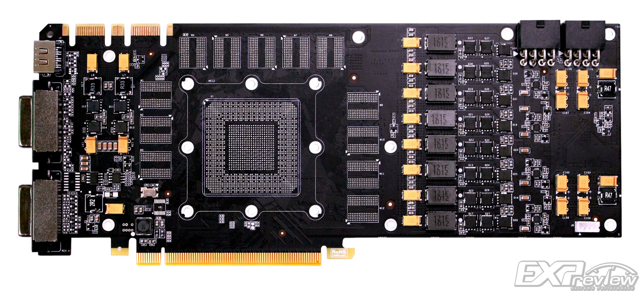
http://bbs.expreview.com/thread-49708-1-1.html

40101961.jpg
 
After reading that post I can't help but think the 950 MHz and $299 rumors were actually disinformation, and the actual numbers are lower for clocks and higher for price.

Since the only other number for clocks I've seen (besides early 3DCenter speculation of ≥ 1 GHz) is 700 MHz, and 3DCenter's estimated prices have gone up to $399, I'm tending to believe those as closer to the real numbers. Or maybe Kyle is actually talking about these numbers….

Since Kyle speaks of planted misinformation from Nvidia, I don't thing they would heighten peoples' expectations, only to deliver something less.
 
I'm guessing this is GK100/110's PCB, with the 6+6+8, 7 phase

edit: for compare
Some early GF100 boards weren't exactly the same as their design diagrams

qso861.jpg


gtx480_11.jpg
 
Last edited by a moderator:
I'm guessing this is GK100/110's PCB, with the 6+6+8, 7 phase
it's 5+2 but +2's phases are weaker.. it's 6+6 pin for axial fan configuration and 6+6/6+8(OC) for vapor chamber+wider blower fan.. tower plug and normal 6 pin plug wont be used at the same time, you wont see them on same pcb..
you wont see something crazy like tower plug(8+6)+6pin
 
Back
Top