NVIDIA Kepler speculation thread

Here is what a New Zealand PC component retailer said a few days ago:

"First shipment of EVGA GTX670 SC has arrived in the country. Supplier has informed us that EVGA have contacted them and placed a recall on those cards - Some sort of fault. It does not look like EVGA will get cards back here until next week. (And it will be the non SC version - so we have been told)"

Thanks. Is it just limited to them?
 
Just for the record:

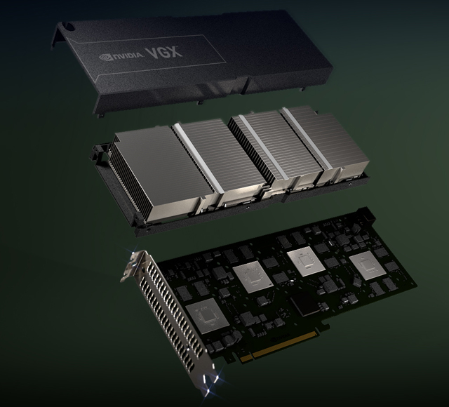
The image of the tesla k10 its from here:

http://www.nvidia.com/object/grid-processors-cloud-games.html

A "NVIDIA® GeForce® GRID Processor" hmmm....

In add.

http://www.nvidia.com/object/vdi-desktop-virtualization.html

http://www.nvidia.com/object/vgx-boards.html

Now it really makes sense to me.

nv-vgx-large.jpg


:D
 
Last edited by a moderator:
I wonder why they are using neutered GK107 dies for the product, rather than fully enabled ones.
If tdp is a problem then they could (further) underclock them.
Or do Nvidia plan a native 192 shader GK108 die.

Just for the record:

The image of the tesla k10 its from here:

http://www.nvidia.com/object/grid-processors-cloud-games.html

A "NVIDIA® GeForce® GRID Processor" hmmm....

In add.

http://www.nvidia.com/object/vdi-desktop-virtualization.html

http://www.nvidia.com/object/vgx-boards.html

Now it really makes sense to me.


:D
 
where can we see GK107 specs?, that idea of a neutered down chip has surfaced, either for the VGX card or for the gt 630 OEM, but in the beginning I just assumed the full chip had 192 units.

any way the thing is for displaying windows aero, google earth, some CAD and 3D modelling or visualisation etc. i.e. things that make very little use of pixel shaders.
I guess you are likely to be ROP and bandwith limited when using it for many display surfaces.
 
Do note that 1Tflops double precision mentioned in the PDF is not peak performance for K20...

We dont have the number right now, it is just what was describe by Nvidia, it could end pretty higher of that .. But we will need to wait for know it. There's no real number about K20.... just some approximative idea of the performance given by Nvidia ( a bit early for write the perf in stone )
 
Last edited by a moderator:
I wonder why they are using neutered GK107 dies for the product, rather than fully enabled ones.
If tdp is a problem then they could (further) underclock them.
Or do Nvidia plan a native 192 shader GK108 die.
Can anyone measure the dies (packages) shown in that VGX picture above? If it ends up around 120-130 mm^2 then it's GK107, if it's considerably smaller then it could be GK108….
 
You are right, it really looks like a GK104. Do they have so many partially defect GK104 chips? Is there some problem with GK106? What other reasons can one think of?
I mean it should be cheaper (and probably more power efficient) to use a GK106 instead of a GK104 with half of the SMXs deactivated to get that kind of performance.
 
You are right, it really looks like a GK104. Do they have so many partially defect GK104 chips? Is there some problem with GK106? What other reasons can one think of?
Maybe GK106 isn't any more problematic than GK104/GK107, but is simply planned for a later release (which admittedly could be a problem in itself if it wasn't strategically planned) and so they had to use a GK104 for the top of the 600M line until then. That doesn't mean there aren't big issues with the GK104 in terms of defects etc. though. Assuming GK106 isn't terrible in efficiency it should be able to match a half CC disabled GK104, if not beat it. I wouldn't be surprised if something like the 480M to 485M transition happens once GK106 arrives.
 
Back
Top