Well my interpretation of the quote is that they can use either 4 or 8 gddr5 memory chips and still have a 192bit bus. But if you have only 4 chips, each chip is only 32bit wide, so there's just no way this will give you a 192bit bus, period.There is completely nothing impossible about this, combination of different density mem's chips could easily solve problem
Install the app
How to install the app on iOS
Follow along with the video below to see how to install our site as a web app on your home screen.
Note: This feature may not be available in some browsers.
You are using an out of date browser. It may not display this or other websites correctly.
You should upgrade or use an alternative browser.
You should upgrade or use an alternative browser.
NVIDIA GF100 & Friends speculation
- Thread starter Arty
- Start date
Not necessarily, if the memory controller is flexible enough. You could for instance imagine that high-bandwidth consumers like back and depth buffers are split up evenly in tiles among all 3 memory partitions, but less bandwidth intensive things (like compressed textures) get split uneven - so for four tiles one tile each to the memory partitions with less memory and 2 tiles to the one with more memory. Sounds too complicated to me though.So.. we have 6 32 bit chips, 4 of them are 1 gbit and 2 are 2 gbit.
Doesn't this mean 192 bit access to the first 768mb ... and useless 64 bit access to the last 256?
Not necessarily, if the memory controller is flexible enough. You could for instance imagine that high-bandwidth consumers like back and depth buffers are split up evenly in tiles among all 3 memory partitions, but less bandwidth intensive things (like compressed textures) get split uneven - so for four tiles one tile each to the memory partitions with less memory and 2 tiles to the one with more memory. Sounds too complicated to me though.
There's 3 separate memory controllers, not one big, though?
Don't know how much that changes how they can work.
It's unlikely that addresses are assigned in big chunks to memory chips because then you can't use the available bandwidth if all objects are allocated to the same address block. It's much better to have fine grained interleaving: 256 bytes to chip 1, 256 bytes to chip 2, etc. So you spread around the accesses evenly to different chips and ensure peak BW no matter how you allocate objects.Psycho said:So.. we have 6 32 bit chips, 4 of them are 1 gbit and 2 are 2 gbit.
Doesn't this mean 192 bit access to the first 768mb ... and useless 64 bit access to the last 256?
But I don't know how that would work in a case of chips with different memory sizes...
According to rumors GTX590 will be released, or at least announced, tomorrow at PAX.
Sweclockers leaked claimed specs for the card http://www.sweclockers.com/nyhet/13618-geforce-gtx-590-lanseras-den-22-mars
2x full GTX580 chips, 3GB mem, 375W TDP
Clocks 60xMHz/15xxMHz/3400MHz
Member at MuroBBS tested his GTX580 at those clocks, and reported on average 22% performance drop for single card, which would indicate that the card would end up slower than HD6990 at default clocks.
You've got a typo there shader clock is 12xx.According to rumors GTX590 will be released, or at least announced, tomorrow at PAX.
Sweclockers leaked claimed specs for the card http://www.sweclockers.com/nyhet/13618-geforce-gtx-590-lanseras-den-22-mars
2x full GTX580 chips, 3GB mem, 375W TDP
Clocks 60xMHz/15xxMHz/3400MHz
Hmm it shouldn't be that slow. Granted with these specs it should be slightly below GTX570 SLI but not by much (it has a bit more memory bandwidth but a bit less shader power despite more SPs due to clock difference). Granted might be quite similar in performance compared to HD6990.Member at MuroBBS tested his GTX580 at those clocks, and reported on average 22% performance drop for single card, which would indicate that the card would end up slower than HD6990 at default clocks.
If the low clocks are true it is actually quite possible this honors the 375W TDP limit - power consumption should definitely stay a bit below GTX 570 x 2.
Yep, typo, good thing i threw the link thereYou've got a typo there shader clock is 12xx.
Hmm it shouldn't be that slow. Granted with these specs it should be slightly below GTX570 SLI but not by much (it has a bit more memory bandwidth but a bit less shader power despite more SPs due to clock difference). Granted might be quite similar in performance compared to HD6990.
If the low clocks are true it is actually quite possible this honors the 375W TDP limit - power consumption should definitely stay a bit below GTX 570 x 2.
Tweaktown did some benches with 580 at 480 clocks (9.2% core drop, 7.8% mem drop)
http://www.tweaktown.com/articles/3...geforce_gtx_580_at_gtx_480_clocks/index3.html
Performance drop at 1920x1200:
Unigine: 9.5%
RE5: 6.3%
HAWX: 6.8%
Mafia 2: 10.4%
Lost Planet 2: 8%
AvP: 8.6%
FF XIV: 8.4%
SF5: 9.6%
FarCry2: 6%
Batman: +5.1% (yes, something definately borked here, lower clocks but higher perf)
With AA enabled:
Mafia: 10.4%
AvP: 10.6%
SF5: 9.4%
FarCry2: 9.8%
With AA all lost more than either core or memclocks dropped, without AA 3 games lost less than mem clocks dropped, 3 games less than core but more than mem, 3 games more than core or mem dropped.
And then there's batman which result has to be screwed up.
onethreehill
Newcomer
Great card!
Much more useful than the 590 and 6990 will ever be. Obviously better priced, with enough performance to tackle the heaviest games out there.
460 1GBs cost 140 euros in my country and I live in a tech expensive country. So if this baby could be around 300, it would be awesome.
DuckThor Evil
Legend
Wonder why they used a 460 instead of a 560.
2x560 would probably be too close to stock/underclocked 590 creating some weird pricing havoc among other things. Curious to see how much this will retail, using older chips, should help this be more affordable, but still having great performance, it should also have pretty decent OC headroom.
It's most likely gf114 chips anyway, but running at 460 clocks to keep power in check (and to differentiate from the 590). So maybe nvidia demanded the 460 name.
But cards like this should have more than 2*1 gb. And I don't see it at 300, considering the low volume, expensive layout, price pressure at the performance point etc.
Galaxy has more or less (but not quite) the same btw: http://en.expreview.com/2011/03/10/...rce-gtx-460-graphics-card-surfaced/15272.html
http://plaza.fi/muropaketti/artikkelit/naytonohjaimet/ennakkokatsaus-nvidia-geforce-gtx-590
Muropaketti tested how GTX 590, if sweclockers clocks are correct, should perform by using 2 GTX 580's. According to Sampsa Kurri, his sources indicate that the reported clocks would be correct ones.
The article is in finnish, but images should be understandable for everyone
The "simulated 590" used a lot more power ( 92 watts more than system with 6990 in dirt 2), but of course at least power consumption figures aren't the same for 2 SLI'd cards and dual chip card, though.
edit: cut out the false part of the post, misread the graphs myself in a hurry
6990 won in 3DMark 11, Crysis Warhead, AvP and Metro 2033, while simulated GTX 590 won Dirt 2 and BFBC2
Last edited by a moderator:
Man from Atlantis
Veteran

Last edited by a moderator:
Man from Atlantis
Veteran
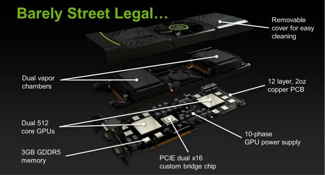
They finally got rid of nF200? At least the shape of the heatspreader on bridge chip suggests it's not nF200 which is quite rectangular, not square.
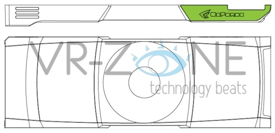
looks same as placed on Galaxy's 460x2.. I see more Galaxy spirit there like removable shroud for easy cleaning and some Gigabyte's ultra durable 2oz copper pcb
Similar threads
- Replies
- 14
- Views
- 2K
- Replies
- 135
- Views
- 6K
- Locked
- Replies
- 10
- Views
- 1K
- Replies
- 0
- Views
- 648

