Install the app
How to install the app on iOS
Follow along with the video below to see how to install our site as a web app on your home screen.
Note: This feature may not be available in some browsers.
You are using an out of date browser. It may not display this or other websites correctly.
You should upgrade or use an alternative browser.
You should upgrade or use an alternative browser.
Nvidia BigK GK110 Kepler Speculation Thread
- Thread starter A1xLLcqAgt0qc2RyMz0y
- Start date
-
- Tags
- nvidia
I believe they aim thoses cards at a certain client type... for the real Tesla deal, you will need to wait. ( something who start to look a bit redundant ). In certain way they will comble the lack of performance in some case ( DP mostly ), by using a dual gpu. Not sure how will be the impact in computing community. ( All depend your needs anyway ).
Given that Kepler GPU architecture increased the amount of SP FLOP from 64 to 96 in a single cycle, we understand the market demand for SP. While HPC customers will probably opt to wait for GK110-based Kepler boards, there is a large amount of customers that said that they don't give a "rat's behind" for DP and that they demand a Kepler part for their computational needs.
Last edited by a moderator:
A1xLLcqAgt0qc2RyMz0y
Veteran
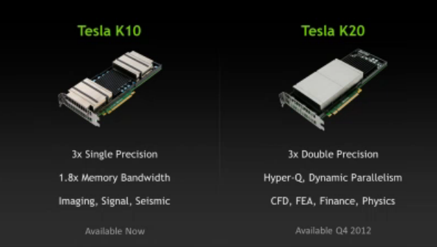
Nvidia Tesla K10
http://www.eetimes.com/electronics-news/4372936/Nvidia-upgrades-Tesla--eyes-cloud-gaming
http://www.eetimes.com/electronics-news/4372936/Nvidia-upgrades-Tesla--eyes-cloud-gaming
Nvidia packs two Tesla K10s on a single PCI Express Gen 3 board to deliver 4.58 teraflops of single-precision floating point performance and 320 gigabytes per second of memory bandwidth.
They support ECC memory and parallel programming models such as the message passing interface (MPI) and are cooled by server chassis subsystems.
The Tesla chips are based on the same 28 nm Kepler core Nividia announced for consumer graphics chips in March. It sports 1,536 Nvidia proprietary Cuda rendering cores and 192 control logic cores on a GHz clock. That’s up from 512 and 32 cores in the 40 nm Fermi parts that ran at 772 MHz.
A1xLLcqAgt0qc2RyMz0y
Veteran
K20?
Well the rumored BigK (GK110) with 7 billion transistors turns out to be the dual K10 (GK104). 2 x 3.5 billion = 7 billion.
So we seem to be back to square one in that we really do not know what the GK110 will offer.
So please post whatever rumors you find on the K20.
Well the rumored BigK (GK110) with 7 billion transistors turns out to be the dual K10 (GK104). 2 x 3.5 billion = 7 billion.
So we seem to be back to square one in that we really do not know what the GK110 will offer.
So please post whatever rumors you find on the K20.
4.58 TFlop/s with two GK104 equals a clock of ~745 MHz. Or if they used the salvage versions with 1344 SPs per GPU it comes out as ~852MHz. That's probably needed to stay comfortably in the 250W(?) TDP.
All in all it doesn't look very convincing to me. Performance per GPU will very likely be a bit lower on average compared to an M2090 flavoured GF110 (and added effort is needed to achieve good scaling if it is feasible at all due to the higher number of GPUs). And you have just 4 GB memory per GPU (instead of 6 GB). And DP performance is just miserable. The only real advantage is the significantly higher single precision performance/Watt, which comes with quite some drawbacks.
Let's hope GK110 is still on track for Q3/Q4 introduction as Tesla K20 to please the crowd waiting for it. This dual GK104 can't replace it.
Blazkowicz
Legend
this means vastly cheaper flops when you rack it up and have to power and cool them 24/7.
well my cfx setup have 7.58 Tflops of SP and ~ 2 TFlops on DP ..
a single 7970 will get 3,79 TFlops on SP and ~1 TFlops on DP .. ( stock clock ofc, cant compare with a Pro version )
I like the idea of dual card... but, im not really convinced. on paper, and TDP wise on small client, maybe, but on large client ? ( they speak about 75 Tflops ...).
a single 7970 will get 3,79 TFlops on SP and ~1 TFlops on DP .. ( stock clock ofc, cant compare with a Pro version )
I like the idea of dual card... but, im not really convinced. on paper, and TDP wise on small client, maybe, but on large client ? ( they speak about 75 Tflops ...).
Last edited by a moderator:
Blazkowicz
Legend
this thing is enterprisey anyway, you pay through the nose next to buying motherboards and gaming cards, stacking tables on top of each other with rows of PC cheap PC cases and using some home or office A/C hardware.
I would like datacenters to look like that. no more crazy SAN and "storage solutions" either just use PCs. but for some reason companies like more expensive and neater things. space and cooling costs become significant, you need someone to blame, and high levels of support (commercial, software and dev tools, availability of parts)
I would like datacenters to look like that. no more crazy SAN and "storage solutions" either just use PCs. but for some reason companies like more expensive and neater things. space and cooling costs become significant, you need someone to blame, and high levels of support (commercial, software and dev tools, availability of parts)
A1xLLcqAgt0qc2RyMz0y
Veteran
4.58 TFlop/s with two GK104 equals a clock of ~745 MHz. Or if they used the salvage versions with 1344 SPs per GPU
You are forgetting that enabling ECC reduces bandwidth and that is probably why it is 4.58.
Bandwidth should do nothing for peak flops.You are forgetting that enabling ECC reduces bandwidth and that is probably why it is 4.58.
( Autocad etc ), this could make an excellent base with lower cost/year.
hmm? autocad uses GPGPU? I don't remember that - and even if it'd use it, you'd be hitting a wall since autocad uses all FP64 geometry...
Blazkowicz
Legend
CAD programs even use a mathematical simulation, inherently single-threaded where every step depends on the preceding step. other parts of the program (modelling, display etc.) can be multithreaded.
then, a Quadro 600 can be well enough, depending on what you're doing. so I guess that Autocad costs much more than the computer needed to run it.
now if you have plugins or other programs that do fluid, heat simulation or something like that it's another story and you could need the 75 teraflops rack sooner than later .
.
drawing simple plans, etc. your old cell phone would be powerful enough. computing is so schizophrenic, it used to be more simple. i.e. want to do CAD, raytracing, 3D games etc.? buy a 486 DX/2 66. you can't get a bigger PC and slower ones are unusable.
then, a Quadro 600 can be well enough, depending on what you're doing. so I guess that Autocad costs much more than the computer needed to run it.
now if you have plugins or other programs that do fluid, heat simulation or something like that it's another story and you could need the 75 teraflops rack sooner than later
drawing simple plans, etc. your old cell phone would be powerful enough. computing is so schizophrenic, it used to be more simple. i.e. want to do CAD, raytracing, 3D games etc.? buy a 486 DX/2 66. you can't get a bigger PC and slower ones are unusable.
Last edited by a moderator:
A1xLLcqAgt0qc2RyMz0y
Veteran
But it does.Bandwidth should do nothing for peak flops.
On the Fermi Tesla's the DP/SP throughput drops when ECC is enabled.
Man from Atlantis
Veteran
K20
Big Kepler (GK110)
The Tesla K20 is based on the GK110 Kepler GPU. This GPU delivers three times more double precision compared to Fermi architecture-based Tesla products and it supports the Hyper-Q and dynamic parallelism capabilities. The GK110 GPU is expected to be incorporated into the new Titan supercomputer at the Oak Ridge National Laboratory in Tennessee and the Blue Waters system at the National Center for Supercomputing Applications at the University of Illinois at Urbana-Champaign.
http://www.marketwire.com/press-rel...-gpus-built-on-kepler-nasdaq-nvda-1657561.htm

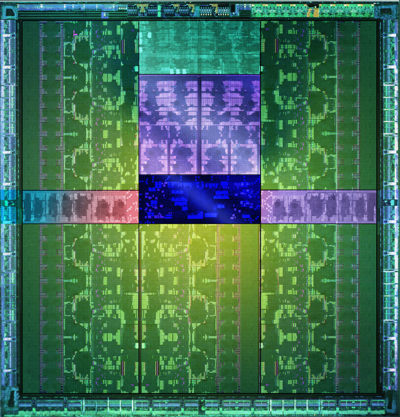
Big Kepler (GK110)

The Tesla K20 is based on the GK110 Kepler GPU. This GPU delivers three times more double precision compared to Fermi architecture-based Tesla products and it supports the Hyper-Q and dynamic parallelism capabilities. The GK110 GPU is expected to be incorporated into the new Titan supercomputer at the Oak Ridge National Laboratory in Tennessee and the Blue Waters system at the National Center for Supercomputing Applications at the University of Illinois at Urbana-Champaign.
http://www.marketwire.com/press-rel...-gpus-built-on-kepler-nasdaq-nvda-1657561.htm
Man from Atlantis
Veteran
Man from Atlantis
Veteran
largest and most powerful gpu we've ever built...
wow even bigger than GT200?
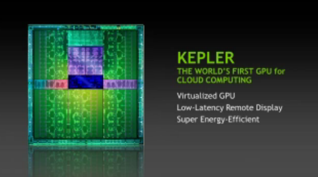
kepler is world's first gpu designed for the cloud, to be deployed into cloud data centers worlwide. it does this with:
--virtualized gpu
--no longer does it need to connect to a display, it can render and stream instantaneously right out of chip to a remote location
--super energy efficiency, so it can be deployed in a massive scale
every command buffer is now virtualized. we can now discern which virtual machine were to send us a graphics command. at the end, we can stream frame buffer to that spsecific virtual machine. one gpu can be shared with countless users
wow even bigger than GT200?

kepler is world's first gpu designed for the cloud, to be deployed into cloud data centers worlwide. it does this with:
--virtualized gpu
--no longer does it need to connect to a display, it can render and stream instantaneously right out of chip to a remote location
--super energy efficiency, so it can be deployed in a massive scale
every command buffer is now virtualized. we can now discern which virtual machine were to send us a graphics command. at the end, we can stream frame buffer to that spsecific virtual machine. one gpu can be shared with countless users
Last edited by a moderator:
Similar threads
- Replies
- 6
- Views
- 4K
- Replies
- 2K
- Views
- 230K
- Replies
- 176
- Views
- 72K
- Replies
- 27
- Views
- 10K

