It varies from card to card a lot, even 100s of MHzs depending on cooling and other factors. And of course, different loads get different boostsI didn't realize they boosted so far beyond their listed clock speeds. I have a gtx1660, but I've never really payed attention to the clocking behaviour.
Install the app
How to install the app on iOS
Follow along with the video below to see how to install our site as a web app on your home screen.
Note: This feature may not be available in some browsers.
You are using an out of date browser. It may not display this or other websites correctly.
You should upgrade or use an alternative browser.
You should upgrade or use an alternative browser.
Nvidia Ampere Discussion [2020-05-14]
- Thread starter Man from Atlantis
- Start date
-
- Tags
- nvidia
DavidGraham
Veteran
My MSI Ventus 2080Ti (maybe the cheapest 2080Ti ever) boosts to 1775MHz all the time.I didn't realize they boosted so far beyond their listed clock speeds. I have a gtx1660, but I've never really payed attention to the clocking behaviour.
D
Deleted member 2197
Guest
Linked an Ampere PDF deck (Inside the Nvidia Ampere architecture) from the GDC 2020 conference dated May 21, 2020.
It covers 4 areas: New Tensor Core, Strong Scaling, Elastic GPU and Productivity.
https://developer.download.nvidia.c...730-inside-the-nvidia-ampere-architecture.pdf
It covers 4 areas: New Tensor Core, Strong Scaling, Elastic GPU and Productivity.
https://developer.download.nvidia.c...730-inside-the-nvidia-ampere-architecture.pdf
My MSI Ventus 2080Ti (maybe the cheapest 2080Ti ever) boosts to 1775MHz all the time.
NV's TF numbers are very conservative for that reason. Almost 1800mhz on a high-end chip like that, damn.
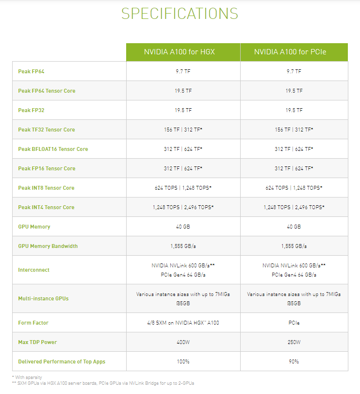
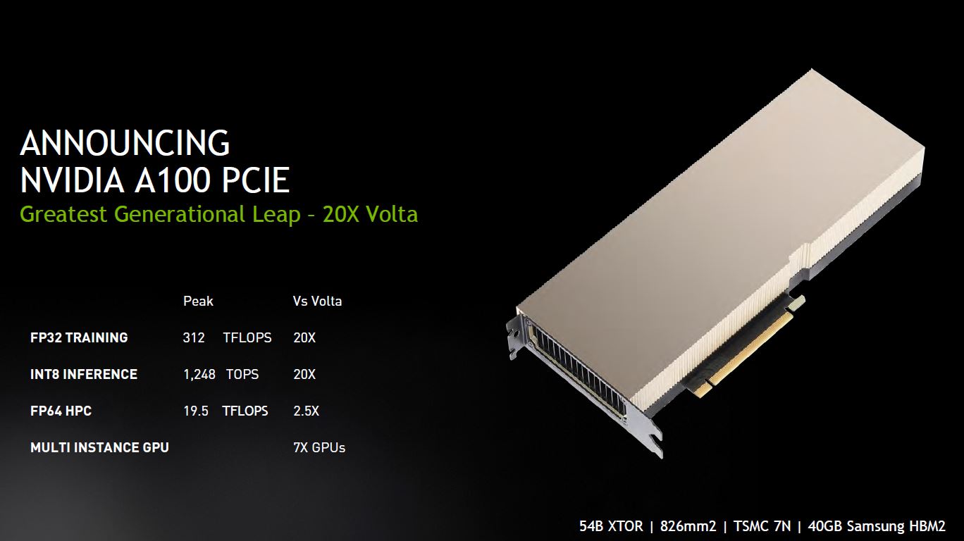
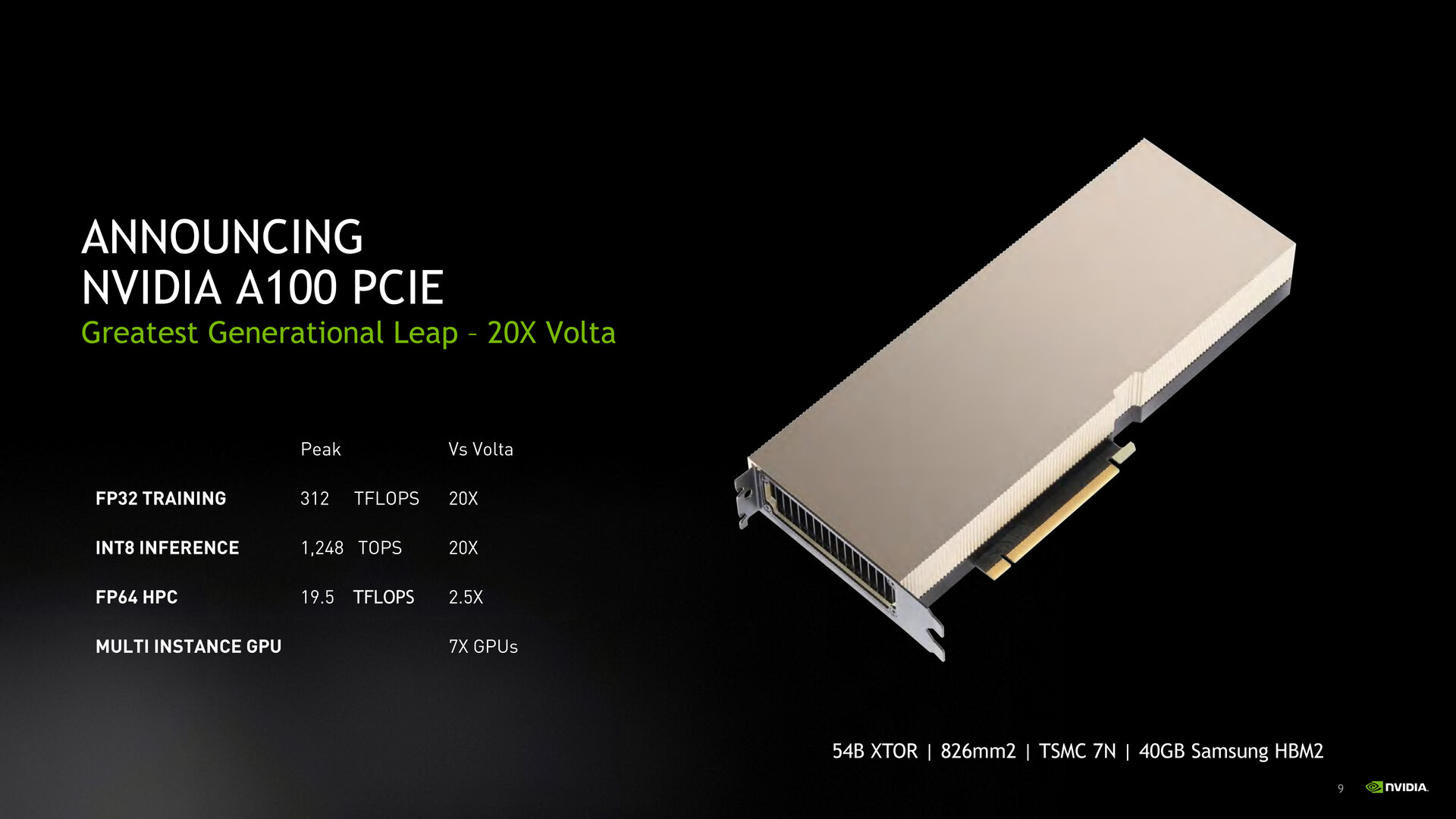
A100 PCIE variant, 250W TDP for %90 performance.
https://www.nvidia.com/en-us/data-center/a100/
https://www.computerbase.de/2020-06/nvidia-ampere-a100-pcie-karte-server/However, there are differences in the TDP, which is set at 250 watts, well below the 400 watts of the SXM4 module. This raises the question of how Nvidia can promote the PCIe card with the same performance values as the SXM4 module. Upon request, Nvidia explained that only the peak performance was identical, but that the continuously (sustained) callable performance of the PCIe card was between 10 percent and 50 percent lower than that of the SXM4 module, depending on the application and configuration of the server.
https://www.servethehome.com/new-nvidia-a100-pcie-add-in-card-launched/
Last edited:
DavidGraham
Veteran
So as explained before, the SXM4 form factor extends power to 400W to accommodate NVLink and higher sustainable clocks, V100 had the same thing happen to it when it extended the SXM form factor to 350W and one more time for 450W.A100 PCIE variant, 250W TDP for %90 performance.
https://www.nvidia.com/en-us/data-center/a100/
D
Deleted member 7537
Guest
https://hardwareleaks.com/2020/06/21/exclusive-first-look-at-nvidias-ampere-gaming-performance/
3080 +30% over 2080TI?
Nvidia doesn't give TF numbers for their consumer cards. For the same reason reviewers don't rely on TF numbers to do their comparisons. Or for the same reason a Radeon VII (14TF) is barely able (in some games) of beating the 2080 (10TF).
3080 +30% over 2080TI?
NV's TF numbers are very conservative for that reason. Almost 1800mhz on a high-end chip like that, damn.
Nvidia doesn't give TF numbers for their consumer cards. For the same reason reviewers don't rely on TF numbers to do their comparisons. Or for the same reason a Radeon VII (14TF) is barely able (in some games) of beating the 2080 (10TF).
Last page called, it wants the link back
Don't be ridiculous, they stopped reporting TFLOPS only when they launched RTX-generation because the new fancy "RTXOps" they invented makes the difference look far bigger than TFLOPS would.Nvidia doesn't give TF numbers for their consumer cards. For the same reason reviewers don't rely on TF numbers to do their comparisons. Or for the same reason a Radeon VII (14TF) is barely able (in some games) of beating the 2080 (10TF).
neckthrough
Regular
It's fair to critique the precision and utility of the specific "RTXOps" metric. However we can't avoid the uncomfortable reality that the utility of raw TFLOPs as a single metric to judge performance is diminishing as chips move towards more specialization in a post-Moore's Law world. Whether it's even possible to come up with a vendor-agnostic and cross-benchmark metric is a tough question. Even "FPS in game XXX" is becoming more challenging due to the difficulty in performing iso-quality comparisons because of divergent feature sets.
D
Deleted member 7537
Guest
Don't be ridiculous, they stopped reporting TFLOPS only when they launched RTX-generation because the new fancy "RTXOps" they invented makes the difference look far bigger than TFLOPS would.
1060, pre-RTX era.
https://www.nvidia.com/en-in/geforce/products/10series/geforce-gtx-1060/
No TFLOPS number to be seen.

DavidGraham
Veteran
All told, the PCIe version of the A100 should deliver about 90% of the performance of the SXM4 version on single-GPU workloads, which for such a big drop in TDP, is not a bad trade-off.
V100 had 4 iterations: PCIe with 250w, SXM2 with 300w, SXM3 with 350w and 450w. The PCIe version delivered lower sustained performance than the SXM versions, but was not documented, this time NVIDIA is documenting this with the A100.
And on this note, I should give NVIDIA credit where credit is due: unlike the PCIe version of the V100 accelerator, NVIDIA is doing a much better job of documenting these performance differences. This time around NVIDIA is explicitly noting the 90% figure in their their specification sheets and related marketing materials. So there should be a lot less confusion about how the PCIe version of the accelerator compares to the SXM version.
https://www.anandtech.com/show/1586...lerator-250w-ampere-in-a-standard-form-factor
The drop is greater in Multi GPU workloads though:
The PCIe 4 variant of the Ampere A100 GPU has a significantly lower TDP of 250W vs the SXM's 400W TDP. Nvidia says this leads to a 10% performance penalty in single-GPU workloads. However, multi-GPU scaling is limited to just two GPUs via NVLink, where NVSwitch supports up to eight GPUs. For distributed workloads, Nvidia says the performance penalty (looking at eight GPUs) is up to 33%.
It appears much of the additional power TDP on the SXM variant goes to inter-GPU communications, based on the 10% performance difference for a single GPU. 400W is also the maximum power limit, so the GPU may not actually use that much in some workloads.
https://www.tomshardware.com/news/nvidia-drops-its-first-pcie-gen4-gpu-but-its-not-for-gamers
Last edited:
Pascal launch, TFLOPS number to be seen1060, pre-RTX era.
https://www.nvidia.com/en-in/geforce/products/10series/geforce-gtx-1060/
No TFLOPS number to be seen.
View attachment 4142

D
Deleted member 7537
Guest
Pascal launch, TFLOPS number to be seen
View attachment 4143
Yep, it was so important that then they decided to remove (well, not even bother to add) that number for the official spec list. NVIDIA does marketing and sells a lot of bullshit they days they announce new hardware, but they know it's not an absolute measure of performance, at least not for gaming.
I was checking and there is not a TF number for even the pascal GPUs. I wonder if NVIDIA decided to stop giving meaningless numbers after the RSX announcement.
Yeah, because the RTX launch definitely didn't see any meaningless numbers on spec sheets...I wonder if NVIDIA decided to stop giving meaningless numbers after the RSX announcement.

D
Deleted member 7537
Guest
Yeah, because the RTX launch definitely didn't see any meaningless numbers on spec sheets...
it just works!
Ampere hasn't fared any better so far, giving big fat numbers which are really big fat lies (like claiming 20x FP32 performance, not telling you that actually they're comparing FP32 of one card to TF32 of Ampere, and others in the similar fashion)Yeah, because the RTX launch definitely didn't see any meaningless numbers on spec sheets...
"big fat lies"? nVidia has published every number for every precision, for example in the whitepaper page 23: https://www.nvidia.com/content/dam/...ter/nvidia-ampere-architecture-whitepaper.pdf
And they have put these litte marks under every comparision, for example here: https://developer.nvidia.com/blog/improving-computer-vision-with-nvidia-a100-gpus/
More open isnt even possible...
And they have put these litte marks under every comparision, for example here: https://developer.nvidia.com/blog/improving-computer-vision-with-nvidia-a100-gpus/
More open isnt even possible...
Should have been more specific, "in their slides", like this:"big fat lies"? nVidia has published every number for every precision, for example in the whitepaper page 23: https://www.nvidia.com/content/dam/...ter/nvidia-ampere-architecture-whitepaper.pdf
And they have put these litte marks under every comparision, for example here: https://developer.nvidia.com/blog/improving-computer-vision-with-nvidia-a100-gpus/
More open isnt even possible...
https://www.computerbase.de/2020-06/nvidia-ampere-a100-pcie-karte-server/
That slide doesn't even have fineprint to remind you to check details somewhere else
Last edited:
D
Deleted member 2197
Guest
Exactly where do they claim a 20x FP32 performance increase when comparing between Ampere and Volta?Ampere hasn't fared any better so far, giving big fat numbers which are really big fat lies (like claiming 20x FP32 performance, not telling you that actually they're comparing FP32 of one card to TF32 of Ampere, and others in the similar fashion)
https://developer.nvidia.com/blog/nvidia-ampere-architecture-in-depth/New TensorFloat-32 (TF32) Tensor Core operations in A100 provide an easy path to accelerate FP32 input/output data in DL frameworks and HPC, running 10x faster than V100 FP32 FMA operations or 20x faster with sparsity.
For FP16/FP32 mixed-precision DL, the A100 Tensor Core delivers 2.5x the performance of V100, increasing to 5x with sparsity.
Tensor Core acceleration of INT8, INT4, and binary round out support for DL inferencing, with A100 sparse INT8 running 20x faster than V100 INT8.
Other reviews had no problems interpreting the graphs along with what Nvidia stated.
https://www.hpcwire.com/2020/05/14/nvidias-ampere-a100-gpu-2-5x-the-hpc-20x-the-training/Benchmarking conducted by Nvidia realized speedups for HPC workloads ranging between 1.5x and 2.1x over Volta (see the “Accelerating HPC” chart further down the page). Peak single precision performance gets a theoretical 10-20X boost with the addition of TensorFloat-32 (TF32) tensor cores.
Similar threads
- Replies
- 49
- Views
- 8K
- Replies
- 98
- Views
- 36K
- Replies
- 1
- Views
- 8K