caboosemoose said:Interesting. Well, in that case, perhaps a G70 clocked over 500MHz might be on the cards.
That's what way too many thought about the NV40.
caboosemoose said:Interesting. Well, in that case, perhaps a G70 clocked over 500MHz might be on the cards.
Jawed said:"Fact" 1: R520 is 295m transistors.
"Guess" 1: R580 is 365m transistors.

Jawed
Ailuros said:Then look back on page2 on caboosemose's comment.

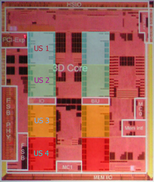
Can't see it.Chalnoth said:That said, you can do the splitting somewhat differently from what you have there and see three groups on the left side, with the two on the right interpretted as the texture pipelines.
The second one would be half above the IO interface, half below. Another way to look at it is that you can split the shader area you highlighted into six equal pieces. Put two into each shader unit and voila.Jawed said:Can't see it.
Jawed
Jawed said:So roughly equating a USA in Xenos to an array in R520, and being generous - I'm guessing an extra 70m transistors for R580.
Ah, but ATI was able to make those ROP's simpler than the ones that you see in today's hardware, because they have much higher memory bandwidth to the memory that they talk to, so they don't have to worry about any sort of compression, for example.Jawed said:If you count 20m transistors for ROP functions on the other die, for 8 ROPs, double that, and add a little more to include compression hardware - say 60m transistors - then Xenos's total logic for 64 pipes, 16 texture pipes and a hypothetical 16 ROPs would be in the region of 300m transistors.
It's not just that, though. It appears that they have done away with the ALU + mini ALU structure (though I'm not 100% certain on that....either way, the next part is true), and their pipelines are certainly less complex, ALU-wise, than nVidia's G70, which has two full ALU's in each pipeline.US pipes in Xenos are simpler than conventional pipes because of the separation of texturing functionality - so assuming that R520/580 use the same separation - then an SM3 pipeline in Xenos is prolly about the same size as an SM3 fragment shader pipeline in R520/580.
Jawed said:Yeah I'm convinced, Chalnoth. Brilliant.
Jawed
Jawed said:As I said earlier:
The assumption that 1 array is given up for yield seems reasonable. The area I've outlined above for the US (should have called them USA, now I think about it, Unified Shader Array) is about 32% of the die, so one US is about 8%.
Jawed
Jawed said:I suspect M$ would choose yield. The extra 16 pipes prolly wouldn't balance very well if the architecture is scaled for 48.
Jawed
Well, just bear in mind that all I'm trying to say is that there are so many variables here, that you should expect to be spectacularly wrong about at least one of the speculations you've made in this threadJawed said:Yeah I'm convinced, Chalnoth. Brilliant.
