Larrabee, console tech edition; analysis and competing architectures

This number is completely wrong though; even a blind man can see that the SPE is not over ten times as long as it is wide! 2.54mm x 5.81mm is the figure I can find.

Yeah, the 3 was added in by accident or some weird copy/pasting from the pdf (it was supposed to be an X, but it got converted to a 3). It's 5.81mm long. :)

FWIW, the XeCPU package is 31mm x 31 mm. I suppose you could try to get a pseudo-dize size measurement looking at this then:

http://www.llamma.com/xbox360/news/inside_the_xbox_360_elite.htm
 
No figure has been discussed to my (limited) knowledge. This is probably all wrong:

XeDie.jpg
 
I still would have made some decisions differently than what Cell did, but that's true in lots of cases.. :) From the link you posted above, it does seem that the idea of local stores and such really did come from the belief that games needed hard real-time requirements. It seems like the set-locking of the Xenon's cache is "good enough" when it comes to that regard (and such real-time certainly isn't needed for HPC).

Cell's PPE also has cache locking, which appears to be a legacy from the POWER architecture. The following quote is from IBM's paper Introduction to the CELL Microprocessor.

The PPE supports a conventional cache hierarchy with 32-KB first-level instruction and data caches and a 512-KB second-level cache. The second-level cache and the address-translation caches use replacement management tables to allow the software to direct entries with specific address ranges at a particular subset of the cache. This mechanism allows for locking data in the cache (when the size of the address range is equal to the size of the set) and can also be used to prevent overwriting data in the cache by directing data that is known to be used only once at a particular set.

http://www.research.ibm.com/journal/rd/494/kahle.html

Its a decent overview of the architecture that goes into the design goals, how they approached those goals, as well as some of the why's of their decisions. It also lists the different programming models that CELL supports.
 
If i remember correctly it was useless according to Capcom.

Look for Zenji Nishbakwa article the one translated

sexy

I don't believe AlStrong's statement was meant to indicate that the cache locking would alleviate the cache thrashing, but was expressing that it was happening despite having it.
 
Was it the guTS project from IBM's Austin Research Lab?

That could very well be it; it seems to be a little earlier than I remember in terms of the timeline, but two-three years ago when it was a hot topic (and many wrongly felt it was a 970 derivative), '97 wouldn't have seemed as distant.

Whatever the case, the origin point is named in a couple of threads floating around here, I just don't have the heart to wade through the thousands of posts to find it. I'm fine to go with guTS though. :) If someone has a correction to make, they'll no doubt do so.

Although I think everyone here (including me) thinks that IBM-->IBM and ATI-->ATI is the most likely move by MS, the truth is that at the minimum, there is a rumor around indicating that Intel may have been in talks with MS late last year to put Big-L in play as a possible component. I've said it before, but I'll say again that it would be a huge win for Intel to get their chip that close to ground zero for DirectX development and into what at the moment has become the default platform for general game development. To the extent that I think they would work very hard to ensure MS that XBox 1-type contract issues wouldn't ever be a concern.

To the topic of Larrabee, I think the question of its viability in the XBox - whether or not it has a business shot of being considered - is a decent microcosm for the architecture in general. Given an architecture capable of scaling to the same extent as a GPU, does its flexibility parlay into an actual advantage over a traditional GPU given a similar die area? And at the time of introduction, what even do we expect a 'traditional' GPU to look like?
 
And Larrabee, for...oh, no particular reason...

aV1NHD79-ec48b2bc8d7e0b39bb8bcdc313e90848.gif


That's Larrabee propose spec from 2006.

The L1 Data and Instruction cache has 1 cycle latency looking at that thing.

Its interesting that each core has its own 256k L2 cache in this early spec.

ArchitectureProfessor described a share cache for Larrabee. When did they change to share cache scheme ? Would that effect the 10 cycle latency mentioned in there.
 
From an IBM paper: The SPE design has roughly 20.9 million transistors, and the chip area including the SMF is 14.8 mm2 (2.54 mm x 5.81 mm) fabricated with a 90-nm silicon-on-insulator (SOI) technology. The 65-nm version of the design is 10.5 mm2.

Impressive. If the Cell SPEs have 20.8 million transistors each, that is only 8.4 million transistors for the logic (after you take away 256KB 6-transistor SRAM cells). That is pretty impressive.
 
When you take a closer look at Xenon it's pretty clear that it was developed in a rush.... Two cycle basic ALU result-forwarding latency, six (!!!) cycle load-to-use latency in the D$ while only hitting 3.2GHz on a state of the art process.

I just looked at the Cell ISSCC paper, they list a 6-cycle load latency for the local store (also running at 3.2 Ghz on the same 90nm SOI process. Granted, the local store is 256KB (whereas the caches on the XeCPU are 32KB, 4-way set associative).

Either way, the compiler/programmer has a pretty big load/use slot to fill on either chip. Of course, the XeCPU has two-threads to hide some of the latency if needed.
 
No figure has been discussed to my (limited) knowledge. This is probably all wrong.

From the figure, that would give a die size of 185 mm^2 for 165 million transistors. That seems in the ball park. Cell is 221 sq. mm for 234 million transistors in the same process. The ratio is a bit different, but that is easily explained by different amount of SRAM vs logic (as well as full-custom layout versus standard cell layout). SRAM is more dense than logic. Full-custom is more dense than standard cells. Cell has both more full custom logic layout and more SRAM.

The end result is that Cell is about 20% larger in terms of die size, but it has 40% more transistors.
 
ArchitectureProfessor described a share cache for Larrabee. When did they change to share cache scheme ?

I don't think I said Larrabee has a shared cache. It does support the "shared memory" programming model, which is different.

Larrabee has per-core (private) L1 and L2s. However, it sounds like they did something to allow fast on-chip cache-to-cache sharing. Something like IBM's "T" state or Intel CSI's "F" state. From what I understand, if the data in anywhere on the chip, the requesting core will get it without the latency of an off-chip DRAM access. So not really a shared cache, but it does do full cache coherence.
 
That's Larrabee propose spec from 2006....
The L1 Data and Instruction cache has 1 cycle latency looking at that thing.

As the clock frequency of Larrabee is half or a third of a high-frequency design of 2009/10 (say 1.25Ghz vs 3.75Ghz), a single-cycle load/use penalty for the cache is plausible (whereas it would be two or three for the 3.75Ghz part).

Its interesting that each core has its own 256k L2 cache in this early spec.

That is still the way it is, from what I've heard. 10 cycles for a 256KB private L2 cache also seems reasonable given the modest clock frequency.
 
If i remember correctly [cache locking] was useless according to Capcom.

Useless meaning: "useless in that it doesn't help prevent cache trashing, so cache thrashing is still a big problem" or "useless in that cache thrashing isn't so bad so we found that set locking didn't help much". Honest question.

I suspect you mean the former, but the latter is also a possibility. Or perhaps a little of both.
 
I just looked at the Cell ISSCC paper, they list a 6-cycle load latency for the local store (also running at 3.2 Ghz on the same 90nm SOI process. Granted, the local store is 256KB (whereas the caches on the XeCPU are 32KB, 4-way set associative).

Either way, the compiler/programmer has a pretty big load/use slot to fill on either chip. Of course, the XeCPU has two-threads to hide some of the latency if needed.

Well, six cycles fits fine with the instruction execution latencies of the SIMD instructions, so you would have to inline and loop unroll your kernels anyway.

Cheers
 
Useless meaning: "useless in that it doesn't help prevent cache trashing, so cache thrashing is still a big problem" or "useless in that cache thrashing isn't so bad so we found that set locking didn't help much". Honest question.

I suspect you mean the former, but the latter is also a possibility. Or perhaps a little of both.

That's what I was wondering too. But in the context of that thread (heh :p), the cache locking appeared to be useless with regards to the eDRAM framebuffer tiling.

Giving that this was bulleted in the context of tiling, I think this was already known. I forget the tarty name MS gave to the principle of rendering vertex data from the CPU and streaming it directly to Xenos, but this is known not to work with tiling - the processing need to be recalcuated per tile.

But then...

you mean that trick with feeding the gpu directly from L2 cache? IIRC for it it was essential to lock cache.
Hence the remark about cache locking being "useless".
Anyway designing a renderer around tiling does introduce extra complexities and considerations you otherwise don't need to make - which makes me wonder if that's actually the source of most complaints there (ie. - damn thing doesn't 'just work', we have to reimplement our pipelines for it).

I wonder if we could get an update from the devs on this - if Dave's comment is an absolute "does not work" in hardware or if it's an API/software issue.

And to keep things on topic ... Is that L2 Cache-to-GPU line a particularly useful feature? Could it be implemented easily for Larrabee ?
 
And to keep things on topic ... Is that L2 Cache-to-GPU line a particularly useful feature? Could it be implemented easily for Larrabee ?

It would be useful only if the GPU can consume it immediately. If one is running any sort of buffered commands from previous frame setup, then no, not useful at all. I'd assume that is the problem with tiling as well - you need to feed the GPU back-to-back with the CPU generating stuff PER tile. That kind of tight synchronization is difficult to pull off without major stalling your CPU.
 
I don't think I said Larrabee has a shared cache. It does support the "shared memory" programming model, which is different.

Larrabee has per-core (private) L1 and L2s. However, it sounds like they did something to allow fast on-chip cache-to-cache sharing. Something like IBM's "T" state or Intel CSI's "F" state. From what I understand, if the data in anywhere on the chip, the requesting core will get it without the latency of an off-chip DRAM access. So not really a shared cache, but it does do full cache coherence.

Thanks for the clarification. Well I got kinda confused between information and what's been discussed. I see slides like these (from B3D article)

Image14-big.jpg


Image15-big.jpg


I thought they had change to a unified L2 cache. I guess I was wrong. Do you know any more detail about Intel implementation? I am intrigued how it will scale up because lack of scalability was one of the reason for Cell SPEs doesn't used cache coherence scheme and opted for the DMA model.

It's interesting that the original patent for Cell call for a large pool of on chip memory (64 MB worth if I wasn't wrong and it isn't a cache) that can be shared and partioned between SPEs. In the end it wasn't viable, but I think in the future they might implement something like that.
 
I am intrigued how it will scale up because lack of scalability was one of the reason for Cell SPEs doesn't used cache coherence scheme and opted for the DMA model.

First, some background.

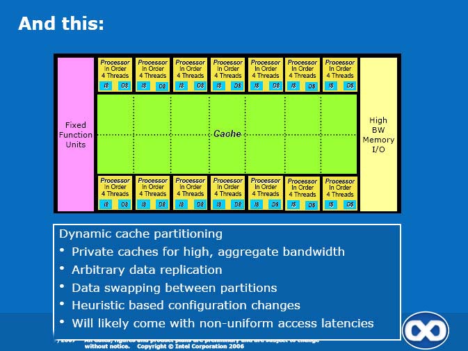
In my opinion, the non-scalability of cache coherence is greatly exaggerated. Yes, connecting hundreds or thousands of processors to make a single cache-coherent shared memory image is really hard (although the SGI Origin did it), but putting a few dozen processors together isn't so bad. Lots of systems have been built by Sun, SGI, IBM, have connected discrete chips. Of course, bandwidth and latency are the issues.

However, once you've moved to an on-chip setting, the latencies go down and the available bandwidth goes up, making building a cache-coherent system even easier. It still isn't easy to design the controller to do it correctly, but even that is becoming easier as we better understand how to build such systems.

Do you know any more detail about Intel implementation?

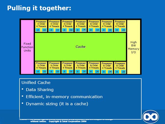
From what I've been told, Larrabee will use a full-map directory protocol. It is conseptually similar to what was proposed in the Stanford DASH prototype and then used in the SGI Origin and Alpha 21364. The difference is that Larrabee uses a directory cache (on-chip) rather than a in-memory directory (stored in off-chip DRAM).

The a directory protocols with directory caches work in general is that in front of each memory controller is a cache that holds information as to which caches on the chip are caching a block. If one core wants to write the block, it first accesses the directory. The directory sends message to invalidate the other cores that have the block cached. These cores all send an acknowledgement message. Once all the acknowledges have been collected, the original processor can write the block.

By using a directory, the system doesn't need to broadcast requests. More importantly, it avoids needing to have all N-1 processors respond with an acknowledgement (as would happen in a Opteron system, for example).

To make this work, the directory tracks which processors cache which blocks. This means the geometry of the directory needs to mirror the combined geometries of the cache tags. In essence, you end up with a highly set-associative cache to hold the directory information (which isn't so good, but can be done).
 
Back
Top