
You are using an out of date browser. It may not display this or other websites correctly.
You should upgrade or use an alternative browser.
You should upgrade or use an alternative browser.
Engineering: What qualities make something great or a mess? *spawn from XBox One X*
- Thread starter MrFox
- Start date
...
Motherboard is still a mess.
How so?
Seeing how it works here (the rise of the MSVU), my post wouldn't be allowed by the mods so I will respect their bias.How so?
But I find integration as fascinating as cooling.
Seeing how it works here (the rise of the MSVU), my post wouldn't be allowed by the mods so I will respect their bias.
But I find integration as fascinating as cooling.
Wrong.
We'd truly would like a genuine post / mini-article as to what makes something solid or something trash with respect engineering. This will now be spun off to it's own thread so everyone is free to answer.
No you don't, as can be seen by all the bullshit comparisons with baseless claims you let pass. I can make a significant effort reading back datasheets and application notes to make sure I remember a bit on a topic... and gibberish statements are equally accepted. It's not the content you accept it's the illusion of it. Even the shit that takes 10 seconds to google and figure out it's FUD.Wrong.
We'd truly would like a genuine post / mini-article as to what makes something solid or something trash with respect engineering. This will now be spun off to it's own thread so everyone is free to answer.
I do as well! This is one reason I find hardware teardowns so fascinating, especially by companies who put as much care into their interior hardware design as much as they do the exterior visual design, such as Sony and Apple.But I find integration as fascinating as cooling.
Please, share your thoughts on this topic, I for one would be very interested to read them.
Cheers!
Now I'm not as well versed as others in engineering or electronics beyond the basic 101 level, but here's my uninformed perceptions anyways.... While I think the Xbox One X motherboard is slightly better than the Xbox One S, but it's only because it's smaller -- it doesn't look as "clean" as it likely should be since it still has oddly placed (oddly used?) capacitors and a lot of SMD chips (for voltage/signal buffers?) in various spots.
For References, I'll try to add in references to the parts in the Xbox One, Xbox One S, and Xbox One X motherboards. It might be tougher finding quality images for some of these. I'll edit in better pictures if/when I can find them.
Xbox One X Front:

/cdn.vox-cdn.com/uploads/chorus_asset/file/9249801/tpina_08082017_1906_0134.jpg)

Xbox One X Back:
Xbox One S tear down: https://www.ifixit.com/Teardown/Xbox+One+S+Teardown/65572
Xbox One S Front:


Xbox One Day-One TearDown: https://www.ifixit.com/Teardown/Xbox+One+Teardown/19718
Xbox One Day-One Front:

Xbox One Day-One Back:

For References, I'll try to add in references to the parts in the Xbox One, Xbox One S, and Xbox One X motherboards. It might be tougher finding quality images for some of these. I'll edit in better pictures if/when I can find them.
Xbox One X Front:
Xbox One X Back:
Xbox One S tear down: https://www.ifixit.com/Teardown/Xbox+One+S+Teardown/65572
Xbox One S Front:
Xbox One Day-One TearDown: https://www.ifixit.com/Teardown/Xbox+One+Teardown/19718
Xbox One Day-One Front:
Xbox One Day-One Back:
Tkumpathenurpahl
Veteran
Seeing how it works here (the rise of the MSVU), my post wouldn't be allowed by the mods so I will respect their bias.
But I find integration as fascinating as cooling.
MSVU = Microsoft Vasectomy Unit?
OG Xbox One should have been a hot mess. I think IIRC you managed to prove it when compared to PS4. Cooling as well.
You were right about it. It was rushed and the external power brick was a resulting factor, they did not have enough time to make it work together and that was the result. IIRC I was on the side thst Xbox was better engineered, by default I lost that argument. What came to be in reality however, was slightly different than you predicted.
I'm am curious though, considering the difference MS had with time with 1X if there was any change (we can see with cooling there is).
VictimsMSVU = Microsoft Vasectomy Unit?
Lol
How would you jump to that lol

I don't even know what I should be looking for here...
Me neither, which is why I am wanting this to be a real topic with real learning points. Perhaps we can get additional insights from those with engineering experience to share with the rest of us.
I'm not sure why they feel like this is a trap and are unwilling to share.

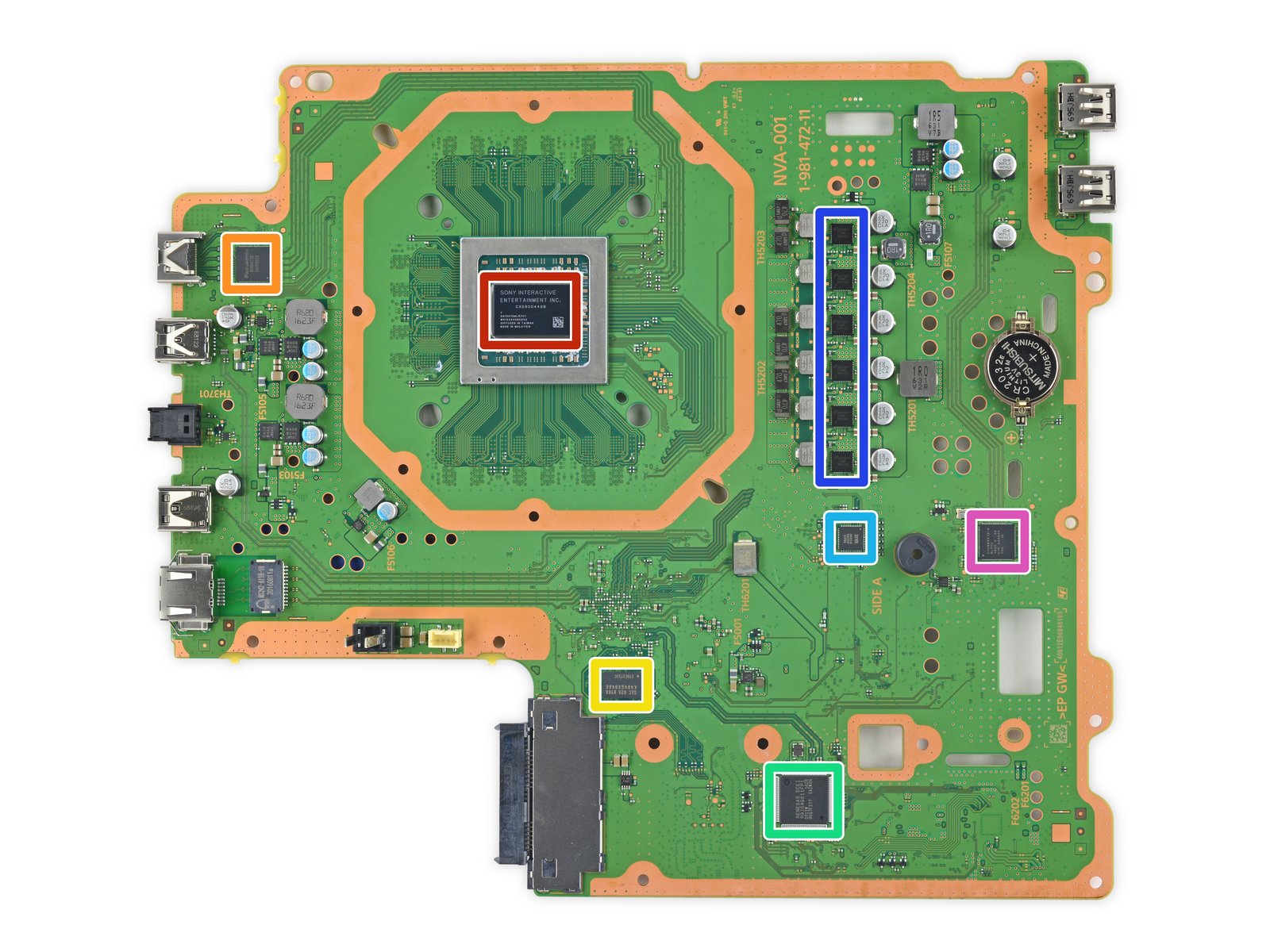
Everything is relative, It's a mess compared to some others console motherboard, like this one (that has similar specs & power consumption):
Taken Pro's teardown.
Can you please share what portions make it a mess on the Xbox One X motherboard, is it the power regulation, the overall layout, or the excessive number of surface mount device components? To this layperson, the 4Pro board looks "cleaner" / less cluttered. I hope that makes sense. Why are there so many additional components on the Xbox One X?
I don't think alot of people give proper acknowledgement to the fact Sony is primarily a hardware company and have 50 years of history designing semiconductor based electronic devices, of course Playstation have had the hardware design edge over Xbox generation after generation after generation (I'd catalogue HIGH performance microprocessor architecture design seperately as Sony ventured into that in the early 90s) and that 50 years is also reflected in their more streamline and elegant motherboards. Look at the OG Xbox (2001) was basically a computer in a box, the 360's RROD, the X1's huge chassis and external power supply on a device that creates less heat than a standard PS4, and PS4 and PS3's more elegant centrifugal cooling solution which MS in Nov 2017 has only started to implement.
Just like MS being a software and OS company, has the edge with their OS and more recently their API via their DX12 implementation on XO. But also to be fair the standard Xbox One has a little bit more functionality than PS4 via the HDMI passthrough, Kinect port & accompanying circuitry, 8GB eMMC NAND, and dual wifi chips as opposed to standard PS4's one.
Just like MS being a software and OS company, has the edge with their OS and more recently their API via their DX12 implementation on XO. But also to be fair the standard Xbox One has a little bit more functionality than PS4 via the HDMI passthrough, Kinect port & accompanying circuitry, 8GB eMMC NAND, and dual wifi chips as opposed to standard PS4's one.
Last edited:
The arrangement of the memory on X1X is interesting, as the front and rear memory isn't parallel to the sides of the chip. I don't recall seeing that anywhere before.
Anyone willing to punt a hypothesis out there? Trace length would seem to be the obvious possibility (space savings are minimal), and if so could that be related to keeping a tight window for accesses and keeping latency as low as possible ....?
I know nothing about motherboard layout; but this is the only thing that would make sense to me about it.Anyone willing to punt a hypothesis out there? Trace length would seem to be the obvious possibility (space savings are minimal), and if so could that be related to keeping a tight window for accesses and keeping latency as low as possible ....?
Its one thing for it to be visually pleasing, it's another for it to be high performance and functional.
I am unsure of the high probabilities of a layout being both highly optimized and both visually pleasing as being the same design. Which is why I'm confused as to how some are identifying what is a hot mess as being poor design, even though it could prove some other purpose we are unaware of.
I mean of course i can visually see there are way more components on the Xbox boards, but if you could tell me which components could be removed/replaced with other things I guess you'd have a strong argument that MS was looking to cut costs.
It's pretty common on GDDR5 graphics cards that memory devices on corners are tilted. It's a somewhat weird tilt on that one chip there in the X, but I doubt it's worth putting too much thoughts on why that is without knowing more of what the H/W engineer(s) doing the layout was thinking. You don't have to match trace lengths (at least within reason, I assumeThe arrangement of the memory on X1X is interesting, as the front and rear memory isn't parallel to the sides of the chip. I don't recall seeing that anywhere before.
) with GDDR5, that's why you can squish the memories a lot closer to the ASIC compared to DDR3 used in the original Bone/S.Similar threads
- Replies
- 14
- Views
- 2K
- Replies
- 15
- Views
- 1K
- Replies
- 21
- Views
- 6K