Current Generation Hardware Speculation with a Technical Spin [post GDC 2020] [XBSX, PS5]

Status
Not open for further replies.
Nintendo did it with Switch. There are games (MK11?) that run higher clocks in general (maybe just in handheld mode), and they also added a boost to clocks specific to some games during loading screens. The former has an impact on battery life, the latter may have an impact, but it might also equalize with game time, since you will spend less time loading and more time playing.

Yeah, one of the benefits of using an entirely off the shelf mobile chip is that it comes validated for a big range of clock and power settings. Nintendo had a lot of options that they could tap into without worrying about going out of spec or having some chips fail with settings that were introduced later.

Unless MS have validated their chips for higher frequencies on the GPU it would be too risky to introduce something faster later. If they have, they might be able to introduce variable frequencies if they have all the relevant features on the chip - but I think it's unlikely. Soft disabling, say, 4 CUs and clocking a few percent higher would remove the need for some of the power monitoring stuff, as you'd be able to calculate what was needed to stay within power limits, but again I think this is highly unlikely.
 
I may not be right on a lot of tihngs, but one thing I can be sure of, the next generation of GPUs post RDNA 2 and post Ampere, are on trend to only go even wider, they most certainly won't go narrower.
Navi22 disagrees. It's a mid-range 40CU, highly clocked GPU with a narrower bus than the PS5. Console GPUs are comparable to mid-range GPUs at launch. For a given cost and power budget, Sony chose something similar with PS5, where narrow and fast is a relative statement. This isn't a statement about where high-end PC GPUs are going, rather their preference.
 
RDNA2, for Navi21 has each of its Raster Units capable of rasterising triangles that have coverage ranging from 1-32 fragments:
https://forum.beyond3d.com/posts/2176773/
XSX has Raster Units with RDNA1 capability of triangle coverage up to 16 fragments. With 4 Raster Units x 16 giving 64 fragments per cycle to match its 64 ROPs.

What RDNA2 is doing is taking 4 triangles, but is capable of finer granularity rasterisation for smaller triangles (using 2 Scan Converters per Raster Unit for coarse and fine rasterisation). This produces twice as many fragments from 4 triangles per cycle compared to XSX. RDNA2 is clearly not XSX for Raster Units.
Great post overall, thanks for guiding me through this.

So I didn't get the chance to post there, but typically speaking I don't see any proof of the rasterizers being able to output at 1 pixel per triangle at high performance. The typical rasterizers as of gen operate at 4 pixels per RB, which is where you're getting an optimal value of 16 pixels per triangle. You can force the rasterizer to have smaller than 16 pixels per triangle but you're going to eat heavy penalties in draw small triangles. Unless something is changed, I would like to see the benchmarks on that, as typically single pixel triangles tanks performance greatly using rasterizer hardware. Not to mention your pixel output become abysmal. The RB+ unit of RDNA 2 allows for double pumping which means you can now support 32 pixel triangles at full rate per clock cycle as well and this is an important foot note.

This is 4 triangles per cycle for XSX:

4x1.825 = 7.3 Gtri/sec or billion per second.

Now, XSX has 4 Scan Converters in total across 4 Shader Arrays for rasterisation (from driver leak and triangle throughput above), and maximum triangle throughput is 4 triangles per clock cycle. This is same as RDNA1 and Navi10. You can see the Raster Units containing scan converters below, 4 in total:
Some things I want to point out as the configurations of RBs or rasterizers don't have to follow any particular format either. As long as it works and it can be done, this is often the face of semi-custom. PS5 very well has the exact same setup, and anything with less shader engines would as well.

I think where you might want to consider is that your assumption that there 4 raster units * 4 RBs * 4 pixels. It could very well be 4 raster units * 2 RBs * 4 pixels * 2 for double pumping. So really 32 ROPs, but double pumped to 64. Thus well not RDNA 1 at least. And this choice was to save on silicon while taking advantage of the double pumping. But this could penalize them in specific formats on the front end compared to a proper 64 ROPs.

RE RGT Video: as Per Jayco's summary of it
Next Generation Hardware Speculation with a Technical Spin [post GDC 2020] [XBSX, PS5] | Page 215 | Beyond3D Forum

* PS5's compute unit architecture is pretty much the same as that in the desktop implementation of RDNA 2 and the Series X.
 
Last edited:
Navi22 disagrees. It's a mid-range 40CU, highly clocked GPU with a narrower bus than the PS5. Console GPUs are comparable to mid-range GPUs at launch. For a given cost and power budget, Sony chose something similar with PS5, where narrow and fast is a relative statement. This isn't a statement about where high-end PC GPUs are going, rather their preference.
well having the same is fine. Let me know when the flagship is going more narrow however.
 
Navi22 disagrees. It's a mid-range 40CU, highly clocked GPU with a narrower bus than the PS5. Console GPUs are comparable to mid-range GPUs at launch. For a given cost and power budget, Sony chose something similar with PS5, where narrow and fast is a relative statement. This isn't a statement about where high-end PC GPUs are going, rather their preference.

By the way, in RDNA2 I believe wide means +CUs & +SA. You have a lot of fixed function hardware per SA, adding more CUs doesn't make it wide per se, actually in terms of SA XBSX is as narrow as PS5 but with those units running slower.
 
Navi22 disagrees. It's a mid-range 40CU, highly clocked GPU with a narrower bus than the PS5.

I've not seen what Navi 22's bus is. I'd assumed it was going to be 256-bit, minus the very costly infinity cache. Is it 128 or 192 bit instead?
 
Great post overall, thanks for guiding me through this.
No problem, thanks.
So I didn't get the chance to post there, but typically speaking I don't see any proof of the rasterizers being able to output at 1 pixel per triangle at high performance. The typical rasterizers as of gen operate at 4 pixels per RB, which is where you're getting an optimal value of 16 pixels per triangle. You can force the rasterizer to have smaller than 16 pixels per triangle but you're going to eat heavy penalties in draw small triangles. Unless something is changed, I would like to see the benchmarks on that, as typically single pixel triangles tanks performance greatly using rasterizer hardware. Not to mention your pixel output become abysmal. The RB+ unit of RDNA 2 allows for double pumping which means you can now support 32 pixel triangles at full rate per clock cycle as well and this is an important foot note.
https://forum.beyond3d.com/posts/2177723/
Above is discussion using 2 scan converters per raster unit, a coarse one and a finer one for smaller triangles. I don’t expect high performance for 1 fragment sized triangle, however, I expect better performance than RDNA1. And a step in the right direction.

I'm not up to date on the thread, but there was talk on benchmarks.

Some things I want to point out as the configurations of RBs or rasterizers don't have to follow any particular format either. As long as it works and it can be done, this is often the face of semi-custom.
Yes, sure. Capability at a unit level are building blocks to a variety of configurations. The unit block itself and its capabilities get upgraded over time. We see here differences at the unit block level between XSX and RDNA2.
PS5 very well has the exact same setup, and anything with less shader engines would as well.
I wouldn't be surprised one bit, where PS5s building blocks are around the same CUs as XSX. However, we still haven't seen a detailed block diagram of PS5 like we have for XSX and Navi21.

One other thing that baffles me is that Cerny discussed small triangles in his presentation. But if he doesn't use the RDNA2 Raster Units, then that is a missed opportunity when he had access to it.
I think where you might want to consider is that your assumption that there 4 raster units * 4 RBs * 4 pixels. It could very well be 4 raster units * 2 RBs * 4 pixels * 2 for double pumping. So really 32 ROPs, but double pumped to 64. Thus well not RDNA 1 at least. And this choice was to save on silicon while taking advantage of the double pumping. But this could penalize them in specific formats on the front end compared to a proper 64 ROPs.
XSX has 64 ROPs.

From the earlier Hotchips diagram, the yellow arrow highlights 116 Giga pixels/s:

64x1.825 = 116.8 Gpix/s

The driver leak for XSX/ Navi21 Lite has 4 RBs per Shader Engine. XSX has 2 Shader Engines, so 8 RBs in total. RDNA2 RB+ each output 8 pixels each:

8 RBs x 8 pixels = 64 pixels per cycle, which matches 64 ROPs and XSXs pixel fillrate.

4 triangles per clock x 16 fragments per triangle = 64 fragments per clock to match 64 ROPs.

4 Raster Units and 8 RB+ units align for XSX.

RE RGT Video: as Per Jayco's summary of it
Next Generation Hardware Speculation with a Technical Spin [post GDC 2020] [XBSX, PS5] | Page 215 | Beyond3D Forum

* PS5's compute unit architecture is pretty much the same as that in the desktop implementation of RDNA 2 and the Series X
Okay, thanks. As mentioned earlier, i don't think there's much of a difference between RDNA1 and RDNA2 CUs. They seem to be tweaked for their respective RDNA1 or RDNA2 Raster Units.
By the way, in RDNA2 I believe wide means +CUs & +SA. You have a lot of fixed function hardware per SA, adding more CUs doesn't make it wide per se, actually in terms of SA XBSX is as narrow as PS5 but with those units running slower.
Yes, you can look at it that way. However, workload is computed on wide SIMD units which make up CUs, which is a more appropriate measure.
well having the same is fine. Let me know when the flagship is going more narrow however.
Fast and narrow, or wide and slow are relative terms. You can already see preferences between Nvidia and AMD high-end GPUs.

Look at an RTX3090, it has more than 10000 Cuda Cores, where as AMDs flagship 6900XT has just over 5000 Shader Cores. Nvidia is already wider. Whereas AMD is relatively narrow, but clocks much faster compared to the slower Nvidia flagship.

We already see AMD as fast and narrow, relative to Nvidia being wide and slow.
I've not seen what Navi 22's bus is. I'd assumed it was going to be 256-bit, minus the very costly infinity cache. Is it 128 or 192 bit instead?
You can see the bus widths in the driver leak below.

The num_tccs entry gives you the number of 16bit memory channels.

Navi21 Lite, 20x16 = 320 bit
Navi21, 16x16 = 256 bit
Navi22, 12x16 = 192 bit

Code:
                Property Navi10 Navi14 Navi12 Navi21Lite Navi21 Navi22 Navi23 Navi31
                  num_se      2      1      2          2      4      2      2      4
           num_cu_per_sh     10     12     10         14     10     10      8     10
           num_sh_per_se      2      2      2          2      2      2      2      2
           num_rb_per_se      8      8      8          4      4      4      4      4
                num_tccs     16      8     16         20     16     12      8     16
                num_gprs   1024   1024   1024       1024   1024   1024   1024   1024
         num_max_gs_thds     32     32     32         32     32     32     32     32
          gs_table_depth     32     32     32         32     32     32     32     32
       gsprim_buff_depth   1792   1792   1792       1792   1792   1792   1792   1792
   parameter_cache_depth   1024    512   1024       1024   1024   1024   1024   1024
double_offchip_lds_buffer     1      1      1          1      1      1      1      1
               wave_size     32     32     32         32     32     32     32     32
      max_waves_per_simd     20     20     20         20     16     16     16     16
max_scratch_slots_per_cu     32     32     32         32     32     32     32     32
                lds_size     64     64     64         64     64     64     64     64
           num_sc_per_sh      1      1      1          1      1      1      1      1
       num_packer_per_sc      2      2      2          2      4      4      4      4
                num_gl2a    N/A    N/A    N/A          4      4      2      2      4
                unknown0    N/A    N/A    N/A        N/A     10     10      8     10
                unknown1    N/A    N/A    N/A        N/A     16     12      8     16
                unknown2    N/A    N/A    N/A        N/A     80     40     32     80
      num_cus (computed)     40     24     40         56     80     40     32     80
                Property Navi10 Navi14 Navi12 Navi21Lite Navi21 Navi22 Navi23 Navi31
 
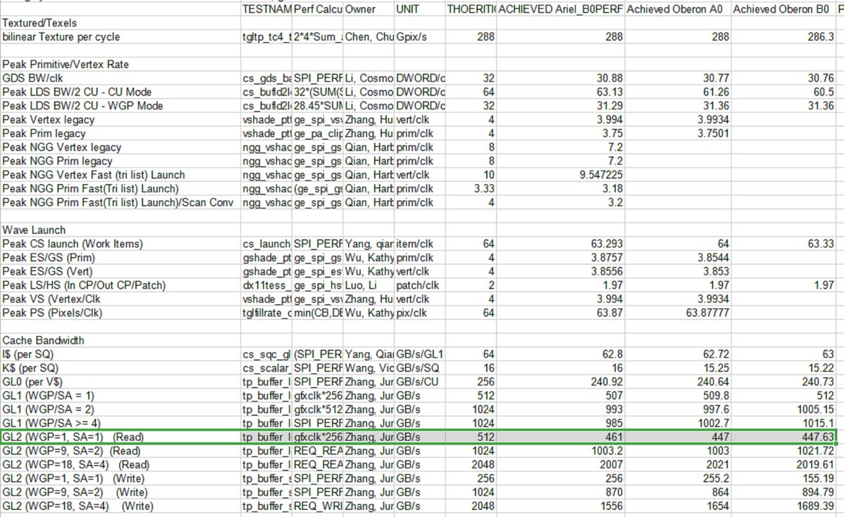
So in terms of hardware there's possibly something going on wrt to L1 or L2 bandwidth, or perhaps the fixed function units and their ability to feed the CUs.
RDNA2 did apparently double the bandwidth of the L2-L1 interconnect, though this probably would apply equally to all derivatives.

My observations over the years are that the amount of compute per pixel and per primitive moves in only one direction. It's unstoppable. This will necessarily cause changes in the way rendering pipelines are stressed. The interesting question is how this will be reflected in console performance as we move through the generation. I think it is more likely to favour XSX (relatively) especially with dynamic clocks in the mix, though I also think it's likely that XSX won't ever match PS5's IPC and show a difference that fully reflects the "TF difference".
Increased CU counts and possibly enhanced throughput for lower-precision math could favor having more concurrent and on average longer-lived shaders, with a possible increase in variety of shader types in-flight. The larger CU count would rely on shaders having longer lifetimes if only because there's a good chance the wavefront launch process scales with shader engine and clock, which is a slower-scaling number. Having more types of shaders being able to coexist can come from having more WGPs and their local caches not being thrashed by too many disparate wavefront types in one place.
Perhaps in the future, an edge in the low-precision throughput might be useful for more aggressive upscaling or reconstruction, and that may also allow for tweaking the burden that RT places on the pipeline. The raw CU count and broader memory subsystem may make some of the penalties of RT traversal and BVH production somewhat less onerous. It would make comparisons more difficult.
The reduction in straightline performance may lead to other parts of the frame taking longer, particularly the spinning up of the broader pixel phase by the frequently narrower geometry setup phase.


I don't think so.
RDNA1:
8qnqV2C.png

RDNA2:
image-136-1536x827.png
In other places, the L1 is indicated as being read-only for coherent data at least. Writes from compute may go out along the path to the L1, but at least for RDNA1 that is for the purposes of flushing whatever line was being written to. The write must go to the L2. One unit that might be bending this rule is perhaps the RBE, but this may be less problematic since it's not considered a coherent client.

It is not to say that the location of the Raster Unit is better or worse, but the change from RDNA1 to RDNA2 is better. And by better means RDNA2 Raster Units can scan convert triangles covering a range from 1 to 32 fragments, with coarse grained and fine grained rasterisation (rather than up to 16 fragments with 1 scan converter with RDNA1):
https://forum.beyond3d.com/posts/2176807/
There was some weirdness about the results that may indicate the relationship isn't that straightforward. Raw pixel throughput might not be so cleanly doubled, since it was claimed some numbers were closer to the more traditional 64 pixels at the front end, versus broader sample throughput at the back end. Hence some references to Fermi's smaller fragment throughput versus ROP throughput. Modes where the same fragment could generate more samples may see more clear scaling.
If the geometry engine itself only outputs 4 non-culled primitives, that would cap the number of rasterizers that could be addressed per cycle.

So, XSX with RDNA1 Raster Units isn't as efficient with shading small triangles (CUs wasting fragment shading cycles by being less efficient). Add this inefficiency with XSX having RDNA1 CUs as well, then your raw Tera Flops are underutilised.
The claim here is that an architecture with 16-wide rasterizers is less efficient at rasterizing small triangles than one with width 32? The big source of inefficiency for rasterizing small triangles comes from the width of the hardware, be it the rasterizer, the SIMD, or RBE. I wonder if the scan converter count means the single RDNA2 rasterizer block is less unified internally.

If PS5 has its Raster Units setup like RDNA2, looking at Navi21 means instead of processing 4 triangles per cycle like XSX, it would drop to 2 triangles per cycle. Because Navi21 with 8 Shader Arrays only rasterises 4 triangles per cycle (halve to 4 Shader Arrays to get PS5). Lower triangle throughput, but higher efficiency of rasterising smaller triangles, with better utilisation from CUs and raw Tera Flops. Your geometry throughput is closer to your lower peak. This was briefly covered in Cerny's presentation about small triangles.
I'm not sure that the PS5 would drop down to 2 triangles. That's a substantial drop in raw capability for geometry, and if sharing RDNA2's organization would cut the number of shader engines--which cuts things like wavefront launch rate as well. The github leak indicated there's 4 triangles per cycle, at least for the types of geometry legacy titles would have. The legacy point would likely matter for backwards compatibility reasons, since it would be more difficult to fake the existence of two missing shader engines for PS4 Pro titles.
Other figures may also point to ~64 pixels/clk for pixel wavefront launch.

The number of shader engines and shader arrays is variable throughout GCN families, so I haven't ruled out a shift in ratios on a per-implementation basis.

Another RGT video.

I think this is the most interesting bits:
  • Sony doesn't want to talk too much about tech after the Road to PS5 talk backlash.
I would have thought technical details could come out in more technical venues, rather than clamp down on technical information because Sony had failed to give the public much else to pick through.

  • The DDR4 chip is for SSD caching and OS tasks, developers will completely ignore this.
This may put some of the earlier rumors to rest about the SRAM-based disk controller, which wouldn't have needed the DDR4 in the first place.

  • Sampler Feedback is missing, saying this is what the Italian Sony engineers meant when he said "It's based on RDNA2, but it has more features and I think one less".
    • He says there are other tools/methods with similar results but harder to implement.
It would be interesting if that feature was the one that wasn't included, particularly since the RDNA2 desktop implementation is supposedly partially defeatured versus the Series X

  • Caches scrubber on the GPU boot invalid or old instructions automatically, freeing up cache space very efficiently and provide improved performance.
Not much detail on what sorts of overheads it is reducing, or what workloads it features heavily in. I'm not entirely sure why it would figure that heavily in instruction invalidation, or that it really frees up cache space. The reason scrubbers would exist is to prevent the equivalent of data corruption rather than free cache space. An invalidated line that is replaced is a net 0 in terms of cache utilization. The danger is if the cache fails to remove stale data and returns it in response to a load.

Navi21 has 8 Shader Arrays and 8 Scan Converters for rasterisation (from driver leak and twice as many as XSX for both), yet its maximum triangle throughput is still 4 triangles per clock cycle, and still has 4 Raster Units as below, where they span Shader Engines rather than Shader Arrays:
Triangle rate by AMD's terms seems to be defined by the capabilities of the Geometry Processor, or whatever shader type might be controlled by it if that's how it works.
 
XSX has 64 ROPs.

From the earlier Hotchips diagram, the yellow arrow highlights 116 Giga pixels/s:

64x1.825 = 116.8 Gpix/s

The driver leak for XSX/ Navi21 Lite has 4 RBs per Shader Engine. XSX has 2 Shader Engines, so 8 RBs in total. RDNA2 RB+ each output 8 pixels each:

8 RBs x 8 pixels = 64 pixels per cycle, which matches 64 ROPs and XSXs pixel fillrate.

4 triangles per clock x 16 fragments per triangle = 64 fragments per clock to match 64 ROPs.

4 Raster Units and 8 RB+ units align for XSX.
Sorry you are correct, I got confused through calculations.
Though not your fault, AMD kept doubling stuff, my brain is swelling from SE, to SA, to dual compute units. Easy to lose track.
The diagrams don't separate what is a shader array in RDNA 2, so it can be easy to forget you're looking at shader engines instead and not shader arrays.

I wanted to point out that the number of RB's from RDNA 1 to 2 were halved. Which I guess wasn't the point you were trying to make; that instead there was 1 primitive unit and 1 raster per SA then per SE therefore the setup is like RDNA 1 and not RDNA 2. Well I'm not sure if that is correct. Because the setup is not likely to define what makes it RDNA 2. Block diagrams aren't necessarily as spot on as listed, how things are connected may not necessarily be as they appear. So it could be 2 rasterizers and 2 primitive units per shader engine. whereas RDNA 2 is 1 rasterizer and 1 primitive unit per shader engine.
If the distinction is that RDNA 1 binds those units to shader arrays than engines, then I would question why that would be a differentiation point or whether that even matters in terms of how it could affect performance. If there isn't something that highlights the difference, I'm not going to think there is any real difference.

In terms of CUs as discussed earlier:
Screenshot_2020-11-18-RDNA-2-questions-areejs12-hardwaretimes-com-Hardware-Times-Mail-1024x557.png


I'm going to go on a limb and say both consoles are 1.1 according to this diagram.
So as you see, it's no different from RDNA 2. I haven't found any other documentation that anything changed from RDNA 1 to 2 exception for mixed precision support and support down to int 4.
So essentially, custom CUs of RDNA 1 became the default for RDNA 2. Of which custom CUs are listed in the whitepaper anyway.

So aside from some speed differentiation in cache transfer. (which may not be necessarily optimal for 2 SE setups) we're not seeing a big difference.
That really just makes RB+ the definitive architectural change between RDNA 1 and 2. And that's really just around double pumping and support for VRS.

So as per this claim:
XSX
Front-End: RDNA 1
Render-Back-Ends: RDNA 2
Compute Units: RDNA1
RT: RDNA

Front End - makes no difference - someone thinking they're smart iwth a block diagram
RBs = RDNA 2
CUs = RDNA 2 or 1.1 which are effectively the same
RT is RDNA 2

So I would disagree with the claim.

edit: sorry I had to bounce around to see your claim here. There's a lot to take in at once, I apologize. It is easy to get lost, I wrote something and had to delete it. the doubling is taking an effect on me.

So basically it comes down to whether PS5 is based off Navi 22 in your opinion. And XSX is based on Navi 21 lite.

That is a very interesting proposition to consider. So you're basically trading off triangle performance to have much higher efficiency at micro-geometry. And because you have fewer triangles to output per cycle, you must rely very heavily on triangle discard.

That could explain things for sure. I need the games to come into my house to test, if the power output is that low, might explain why. It's basically slowing down with micro-geometry and nothing is really happening.

Interesting proposition to say the least.
Okay well we are about 6 months out now so here are some possible explanations for launch game performance as this is getting stale and probably no longer applicable (I would hope things have changed)

Geometry Shader (GS)
• Although offchip GS was supported on Xbox One, it’s not supported on Project Scarlett.
• We’re planning to move to Next-Generation Graphics (NGG) GS in a future release of the GDK.
• Performance for GS in the June 2020 release isn’t indicative of the final expected performance and will be improved in future releases.
• GS adjacency isn’t fully supported in the June 2020 release, but we’ll provide full support in a future release.

• You might encounter some issues with GS primitive ID with certain configurations. Please let us know if you do and the configuration you used so that we can further investigate the issue and provide a fix.
• When using multiple waves in a thread group, you might encounter graphics corruption in some GSs. If you do, please let us know so that we can try to help unblock you.

**
So typically IIRC, geometry shaders are very low performance and I believe most people get around them using compute shaders as the work around. But perhaps they don't suck using NGG. And that might explain why the RDNA 2 cards are performing very well in certain games? Just my thought here. It is likely outperforming a compute shader. Or just NGG in itself has been a big part of RDNA 2 success so far and more so with the titles that are supporting it. It's not exactly clear to me, nor the extent to which XSX can leverage the NGG path.

This is the convo:
 
Last edited:
well having the same is fine. Let me know when the flagship is going more narrow however.
More narrow that what? If AMD release a 90 CU part, how do you know if this was favoured over an alternative 100 CU design at a lower clock speed, or am 80 CU part at higher clock speed?

Compared to its predecessor, AMD have ramped clocks up across the board for RDNA2. Perhaps, like Sony, they like what performance improvements they're seeing at higher clocks and that's why they've banked on investing more in improving the cache (InfinityCache).
 
No problem, thanks.

https://forum.beyond3d.com/posts/2177723/
Above is discussion using 2 scan converters per raster unit, a coarse one and a finer one for smaller triangles. I don’t expect high performance for 1 fragment sized triangle, however, I expect better performance than RDNA1. And a step in the right direction.

I'm not up to date on the thread, but there was talk on benchmarks.


Yes, sure. Capability at a unit level are building blocks to a variety of configurations. The unit block itself and its capabilities get upgraded over time. We see here differences at the unit block level between XSX and RDNA2.

I wouldn't be surprised one bit, where PS5s building blocks are around the same CUs as XSX. However, we still haven't seen a detailed block diagram of PS5 like we have for XSX and Navi21.

One other thing that baffles me is that Cerny discussed small triangles in his presentation. But if he doesn't use the RDNA2 Raster Units, then that is a missed opportunity when he had access to it.

XSX has 64 ROPs.

From the earlier Hotchips diagram, the yellow arrow highlights 116 Giga pixels/s:

64x1.825 = 116.8 Gpix/s

The driver leak for XSX/ Navi21 Lite has 4 RBs per Shader Engine. XSX has 2 Shader Engines, so 8 RBs in total. RDNA2 RB+ each output 8 pixels each:

8 RBs x 8 pixels = 64 pixels per cycle, which matches 64 ROPs and XSXs pixel fillrate.

4 triangles per clock x 16 fragments per triangle = 64 fragments per clock to match 64 ROPs.

4 Raster Units and 8 RB+ units align for XSX.


Okay, thanks. As mentioned earlier, i don't think there's much of a difference between RDNA1 and RDNA2 CUs. They seem to be tweaked for their respective RDNA1 or RDNA2 Raster Units.

Yes, you can look at it that way. However, workload is computed on wide SIMD units which make up CUs, which is a more appropriate measure.

Fast and narrow, or wide and slow are relative terms. You can already see preferences between Nvidia and AMD high-end GPUs.

Look at an RTX3090, it has more than 10000 Cuda Cores, where as AMDs flagship 6900XT has just over 5000 Shader Cores. Nvidia is already wider. Whereas AMD is relatively narrow, but clocks much faster compared to the slower Nvidia flagship.

We already see AMD as fast and narrow, relative to Nvidia being wide and slow.

You can see the bus widths in the driver leak below.

The num_tccs entry gives you the number of 16bit memory channels.

Navi21 Lite, 20x16 = 320 bit
Navi21, 16x16 = 256 bit
Navi22, 12x16 = 192 bit

Code:
                Property Navi10 Navi14 Navi12 Navi21Lite Navi21 Navi22 Navi23 Navi31
                  num_se      2      1      2          2      4      2      2      4
           num_cu_per_sh     10     12     10         14     10     10      8     10
           num_sh_per_se      2      2      2          2      2      2      2      2
           num_rb_per_se      8      8      8          4      4      4      4      4
                num_tccs     16      8     16         20     16     12      8     16
                num_gprs   1024   1024   1024       1024   1024   1024   1024   1024
         num_max_gs_thds     32     32     32         32     32     32     32     32
          gs_table_depth     32     32     32         32     32     32     32     32
       gsprim_buff_depth   1792   1792   1792       1792   1792   1792   1792   1792
   parameter_cache_depth   1024    512   1024       1024   1024   1024   1024   1024
double_offchip_lds_buffer     1      1      1          1      1      1      1      1
               wave_size     32     32     32         32     32     32     32     32
      max_waves_per_simd     20     20     20         20     16     16     16     16
max_scratch_slots_per_cu     32     32     32         32     32     32     32     32
                lds_size     64     64     64         64     64     64     64     64
           num_sc_per_sh      1      1      1          1      1      1      1      1
       num_packer_per_sc      2      2      2          2      4      4      4      4
                num_gl2a    N/A    N/A    N/A          4      4      2      2      4
                unknown0    N/A    N/A    N/A        N/A     10     10      8     10
                unknown1    N/A    N/A    N/A        N/A     16     12      8     16
                unknown2    N/A    N/A    N/A        N/A     80     40     32     80
      num_cus (computed)     40     24     40         56     80     40     32     80
                Property Navi10 Navi14 Navi12 Navi21Lite Navi21 Navi22 Navi23 Navi31
What do you think about some of the github PS5 data in regards to the NGG vertex and primitive performance?

ES7D1jdUUAEi6Zi.jpg
 
More narrow that what? If AMD release a 90 CU part, how do you know if this was favoured over an alternative 100 CU design at a lower clock speed, or am 80 CU part at higher clock speed?

Compared to its predecessor, AMD have ramped clocks up across the board for RDNA2. Perhaps, like Sony, they like what performance improvements they're seeing at higher clocks and that's why they've banked on investing more in improving the cache (InfinityCache).
More narrow than it's predecessor. Effectively you have to compare the high end, as they cut down from there for other product segments.
So if the 4090 is less than 80 CUs, then by all means, I guess going narrow is the way to go.
This wasn't meant to be a controversial statement, bigger than 80CU for the next flag ship is what I expect. I don't care if it's a little larger or a lot larger.
 
Do people actually consider a 80CU part narrow? The XSX is called wide (and slow) by...... everyone basically?
6800> all are wide and very fast at the same time. Ampere products are wide, wouldnt call them slow either.
6700/XT (10.2TF) are going to be narrow/fast, but they are midrange gpus, just like the PS5's. The trend has been going wider with every generation of GPUs going forward, even for AMD's latest RDNA2 GPUs.
 
So if the 4090 is less than 80 CUs, then by all means, I guess going narrow is the way to go.
This wasn't meant to be a controversial statement, bigger than 80CU for the next flag ship is what I expect. I don't care if it's a little larger or a lot larger.
At the high-end you have the luxury of juicier yields to pick, more power, more space and more cooling. This aren't necessarily the case for the performance enveloped of a console. I don't think the new high-end needs to narrower than it's predecessor; you need look at the general trend across recent generations of architecture and compared wide and clocks and see whether this expansion tapers in on those trends or continues. A change in trend is generally a change in behaviour.
 
At the high-end you have the luxury of juicier yields to pick, more power, more space and more cooling. This aren't necessarily the case for the performance enveloped of a console. I don't think the new high-end needs to narrower than it's predecessor; you need look at the general trend across recent generations of architecture and compared wide and clocks and see whether this expansion tapers in on those trends or continues. A change in trend is generally a change in behaviour.
I was explicit in my reference to GPU families. Consoles have strict power envelopes and requirements around pricing etc. The next generation of console could be a handheld or some mobile travelling device for all I know.
I'm strictly talking about the next generation of GPUs.

The only trend right now that I've seen for the last 10 years of GPUs, is the flagship GPU getting larger and if it allows, and it usually does, to run clocks even higher. Even with clocks boosting as high as they are, they take a new node and add more silicon for more power. I've not seem them take a new node keep the chip smaller and run it higher and declare it the flagship.

I have never seen the term narrow and fast really get pushed until this generation of Sony console. It's has always been on trend to go both wider and faster every generation of node change. Even the largest chips can clock significantly higher while being wider than the previous generation while maintaining a similar power envelope.

I was only debating the point that *performance improves* if you get even more narrow and clocks get higher. And GPU chips have always trended towards both larger and faster. This is the first I've heard of this idea that putting in less ALU and increasing the clocks is significantly better opposed to adding more CUs and having a slightly lower clock. The differential between PS5 and XSX in terms of clock speed is not due to size of SoC, but due to one being fixed and one being variable. The difference has exaggerated for the sake of calling one narrow and fast and the other wide and slow. The reality is, 1 is fixed, and one is not.
 
I was only debating the point that *performance improves* if you get even more narrow and clocks get higher. And GPU chips have always trended towards both larger and faster. This is the first I've heard of this idea that putting in less ALU and increasing the clocks is significantly better opposed to adding more CUs and having a slightly lower clock.
Its not about less ALU, it's about finding the right balance, given memory size, bus width, bus clock, cache clock and GPU clocks, or have more more hardware clocked slower or less hardware clocked higher. There's obviously no single right answer to this but it's hard to look at the direction AMD have gone and not notice they're pushing clocks harder than ever. You can't keep going wider indefinitely, signal integrity is already a barrier for XSX according to Andrew Goossen. More silicon will exacerbates that. Mark Cerny also said PS5s CPU has to be limited to 3.5Ghz - which is likely the same issue. Microsoft and Sony are hitting similar barriers to reliability, one though going wide, the other through clocking high.
 
Its not about less ALU, it's about finding the right balance, given memory size, bus width, bus clock, cache clock and GPU clocks, or have more more hardware clocked slower or less hardware clocked higher. There's obviously no single right answer to this but it's hard to look at the direction AMD have gone and not notice they're pushing clocks harder than ever. You can't keep going wider indefinitely, signal integrity is already a barrier for XSX according to Andrew Goossen. More silicon will exacerbates that. Mark Cerny also said PS5s CPU has to be limited to 3.5Ghz - which is likely the same issue. Microsoft and Sony are hitting similar barriers to reliability, one though going wide, the other through clocking high.
Absolutely and on the topic of I think the direction Nvidia has been heading is every bit as valid as AMD going another direction wrt: more dedicated accelerator silicon for Nvidia - cache and clocking for AMD.
I just also can't ignore trend both companies are more than willing to increase everything (Cache, RT Cores, Tensor Cores) to sustain a larger chip, not just increasing the ALU alone.
Chip design will still largely be designed to tackle bottlenecks, I don't think that changes.
 
Absolutely and on the topic of I think the direction Nvidia has been heading is every bit as valid as AMD going another direction wrt: more dedicated accelerator silicon for Nvidia - cache and clocking for AMD.
Yup, this in particular seems to come and go every few years with whatever new technical problem has surfaces. You get trends of bespoke hardware to solve specific problems because the solutions to problems are quite specific to the problem then the main silicon adopts it and implements more generalised hardware to solve those problems while also offering utility in other areas. We've seen this with audio, physics and now RT.

It definitely keeps hardware interesting. :yes:
 
Status
Not open for further replies.
Back
Top