Err, why would they do that when they can just remove it altogether and use software emulation?(which is their plan anyway...)
Uhm cause they are still producing PStwo's? And also, until that emulation is ready, it makes sense to move EE+GS to 45?
Err, why would they do that when they can just remove it altogether and use software emulation?
When did they promise that?... and hopefully the up scaling of all PS2 games to 720p as they had initially promised.
http://www.bloomberg.com/apps/news?pid=20601101&sid=aXr.PBbgNC6Y&refer=japan
Is this a hint? Is April 1st the date they intend to start shipping units with 65nm parts? It seems to tie in nicely with the fact that 65nm Cell production is already underway.
Uhm cause they are still producing PStwo's? And also, until that emulation is ready, it makes sense to move EE+GS to 45?
 ) and the second one: ah, it all makes sense now
 They have hinted at "major changes" to the firmware in time for the European launch.
Of course this could be many things, but in my opinion is likely to be the inclusion of the emulation software and hopefully the up scaling of all PS2 games to 720p as they had initially promised.
Who cares about PS2 scaling, they have a list of things to fix or add before something petty like that. They need a 1080i fix for 720P games, background DLing in the PS store, more PSN demos and arcade games, etc.
I also don't remember Sony ever saying they were going to add features to BC games, it works great now, move on to important things.
In theory, you could consider a node move from 90nm to 65nm to ultimately reduce the cost of a chip by 50%. But in truth it's more complicated than that. The potential savings though are obviously significant however; that's what needs to come through here.
Thanks anyways!My first job at my current company was in the cost reduction group. And I worked a number of our products when they had a die shrink of the main core controller. So I know what happens with these. What I was trying to get is some actual numbers
So if things go well for Sony, they get 65nm Cells, and PS2 emulation so they can drop the EE+GS, saving them a lot more on the hardware just around the European launch...where they charge us the most for the hardware when it's at it's cheapest!Agreed, makes sense.
So if things go well for Sony, they get 65nm Cells, and PS2 emulation so they can drop the EE+GS, saving them a lot more on the hardware just around the European launch...where they charge us the most for the hardware when it's at it's cheapest!
It'd be nice to know when RSX @ 65nm will occur. That'd probably be the ideal early system to get (if price is no concern) as you'll have the coolest, quietest system for a good while.
Although, are smaller processes more or less reliable? This is something that's been concerning me of late, having more high-tech electronic widgets die on me than elder low-tech electronic widgets ever seemed to. Smaller circuitry means less ability to endure wear and tear. Does the lower power consumption mean less wear and tear and 65nm chips will last longer, or do smaller and smaller nodes mean shorter and shorter lifespans for processors?
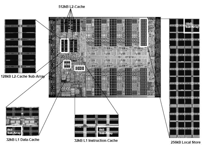
).No, well, that session is about SRAM and not Cell itself contrary to the reports by some media.One, thanks for the die shot. Has there been any news out of ISSCC on the 6GHz/dual-supply Cell session?
No, well, that session is about SRAM and not Cell itself contrary to the reports by some media.
I was hoping we'd get some insights into improved thermal and/or power profiles since that seemed to be a thrust with this.No more details on the site I pulled the pic. Apparently the 65nm Cell pic was briefly shown for 20 seconds to quench those who anticipated too much from the presentationI think we're talking about the same thing, I just wrongly highlighted the processor speed when that was not the central focus of the presentation (though they mentioned it in their blurb on the ISSCC site). I guess rather what I meant was, are their any presentation details containing any of the specifics from the presentation?
they'd manufacture 65nm Cell for consumer appliances. It has 4 SPEs and they plan to remove PPE too. FlexIO may be replaced with a more general interface, but XDR RAM is still necessary for bandwidth..
PPE is not an essential part of Cell. They can use MIPS or whatever they want.If it doesn't have a PPE or main core then it's not really a CELL processor, it'd be a generic DSP of sorts.