ATI MSAA/ eDRAM module patent for R500/ Xenon?

Well, investigating some more on the question of where the sample memory is, I've been rummaging through the associated patent:

Method and apparatus for video graphics antialiasing using a single sample frame buffer and associated sample memory

Basically the patent describes the sample memory, 25, as being "slow" (and big), not necessarily as high-performance as the frame buffer memory, 46.

The patent suggests that the buffer, 20, can be used to hide the latency of fetching sample sets from sample memory.

Jawed
 
Earlier in the thread we briefly touched on the random access bandwidth capability of the EDRAM. The best case appears to be 250MHz for a 90nm EDRAM. How does that translate into the effective bandwidth internal to the EDRAM?


Internal bandwidth depends on internal bus size. Bus size depends on the number memory devices used and the size of the buses for each of the memory devices. Assuming a 2560-bit bus at 250MHz, that's 80GB/s. For reference Flipper in GCN has a 896-bit bus for the eDRAM at 162MHz which gives it 18.1GB/s.
 
Another patent for your reading pleasure not sure if it's already been posted

Combined floating-point logic core and frame buffer

1. An apparatus comprising:

a logic core to provide manipulation of graphical data;

at least one embedded memory unit instantiated on a single substrate with the logic core and coupled to the logic core to perform memory transactions, the memory unit containing both frame buffer memory and texture memory, such that the logic core cooperates with the embedded memory unit to identify a resolution and a mode of a graphical format such that one or more registers are set to indicate a first portion of the embedded unit dedicated as the frame buffer and a second portion dedicated as the texture memory;

It seems MSAA(up to 8 samples?) on fp16 is supported and a z-buffer up to 28bit and a correspending texture format(z28) with(32bit/texel)
 
I don´t believe that we are talking about an eDRAM in the correct term of the word but I can believe that this eDRAM is in the GPU but like the L2 Cache of the PentiumII and PentiumIII Katmai.
 
Urian said:
I don´t believe that we are talking about an eDRAM in the correct term of the word but I can believe that this eDRAM is in the GPU but like the L2 Cache of the PentiumII and PentiumIII Katmai.

What's the point of having 10MB of cache though? :?
 
I am not talking about a cache, sorry, I am NOT a native english speaker and is a possibility that I have told the things wrong.

If you remember the PentiumII the L2 cache wasn´t on the core, it was outside the core but in the same package, Intel used this configuration for PentiumII and the PentiumIII until the Coppermine was released.

I am not talking about a cache, but Imagine that the GPU has 2 modules in it, the first module is the GPU and the second module is the 10MB of RAM, this RAM could be used exclusively for more performance in the GPU because this RAM will be more faster than the main RAM and for some mathematic operations is better a faster RAM.

EDIT: I forgot The NOT. :(
 
Urian said:
I am not talking about a cache, sorry, I am NOT a native english speaker and is a possibility that I have told the things wrong.

If you remember the PentiumII the L2 cache wasn´t on the core, it was outside the core but in the same package, Intel used this configuration for PentiumII and the PentiumIII until the Coppermine was released.

I am not talking about a cache, but Imagine that the GPU has 2 modules in it, the first module is the GPU and the second module is the 10MB of RAM, this RAM could be used exclusively for more performance in the GPU because this RAM will be more faster than the main RAM and for some mathematic operations is better a faster RAM.

EDIT: I forgot The NOT. :(

What you're describing are still two separate chips packaged as a MCM (multi-chip-module)...e.g. IBM Power 5 chips are packaged similarly. It also suits the EDRAM 'module' tag... ;)
 
Jaws said:
Urian said:
I am not talking about a cache, sorry, I am NOT a native english speaker and is a possibility that I have told the things wrong.

If you remember the PentiumII the L2 cache wasn´t on the core, it was outside the core but in the same package, Intel used this configuration for PentiumII and the PentiumIII until the Coppermine was released.

I am not talking about a cache, but Imagine that the GPU has 2 modules in it, the first module is the GPU and the second module is the 10MB of RAM, this RAM could be used exclusively for more performance in the GPU because this RAM will be more faster than the main RAM and for some mathematic operations is better a faster RAM.

EDIT: I forgot The NOT. :(

What you're describing are still two separate chips packaged as a MCM (multi-chip-module)...e.g. IBM Power 5 chips are packaged similarly. It also suits the EDRAM 'module' tag... ;)

Yes, It is.
 
Jawed -

My understanding of the patent is that "sample memory" is external memory. I can't really see it being on die or on the eDRAM block since it potentially needs to hold z/color/stencil data for the entire scene. Maybe a portion of it resides on the eDRAM and is steadily trickled out to main memory as bandwidth permits <- aaronspinks idea...
 
The sample memory would never hold the entire scene. That's the frame buffer's job. The sample memory only holds fragments as long as it's not possible to turn them into completed pixels.

Just to make the patent harder to read :LOL: the patent is written to encompass any anti-aliasing scheme, whether it's super sampling or edge multi-sampling (or... erm dunno!).

If you take the simple case of edge multi-sampling, then the AA samples are encoded in a single bit per sample (they're just geometry samples, so the triangle either covers each sample point or it doesn't). That's encoded as the coverage mask. So on top of the colour and z that you need to hold for the fragment, you only need 1 byte for upto 8xAA samples in the coverage mask.

The other point about edge anti-aliasing, of course, is that you don't need to store a fragment in the sample memory if the fragment isn't on a triangle edge. If that pixel (according to z-testing thus far) is visible then it is blended with the existing value of the pixel in the frame buffer and the fragment is discarded. If the pixel is entirely hidden, then of course the fragment is discarded.

So in edge multi-sampling you're not trying to store anything like the entire frame in the sample memory. You're only storing the fragments that are unresolvable thus far.

A simple way (this isn't the entire method) of defining unresolved fragments relating to a pixel is to consider the coverage mask. In 8xAA, you can't resolve the colour/z of a pixel until all 8 samples have been covered by one or more fragments. So if two fragments only cover 6 of the 8 samples within a pixel, you can't blend those two fragments until you resolve how the final two samples are covered.

As the frame's triangles are rendered as fully resolved pixels, fragments in the sample memory are discarded - so the consumption of sample memory is constantly rising and falling. When the last triangle's last fragment arrives and you process it, you will have resolved all outstanding fragments in sample memory, which means it is empty.

So, after all that, the storage demands of the sample memory are not as seemingly huge as they first appear. At least if using edge multi-sampling.

Why was 10MB chosen for the EDRAM? What are the approximately 3MB of unused EDRAM doing (1280x720x8 is 7MB ish)?

-------

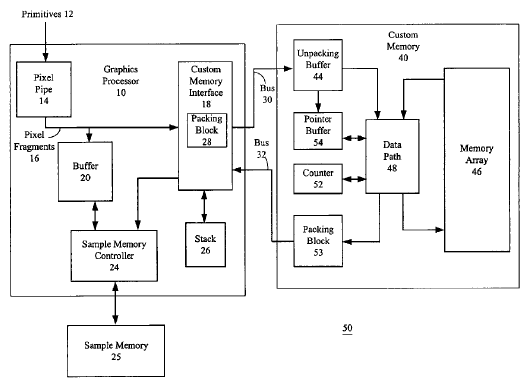
The buffer, 20 in the patent, is designed to hold fragments as they come from the GPU. But it also holds those fragments as they are fetched out of sample memory (or, potentially, on their way into sample memory).

The primary reason for 20 is so that the fragment data can be blocked into compressible units for maximum efficiency as they go over the bus - and also so that the fragment data requires a minimal-cost fetch of pixels from EDRAM by the Data Path blending unit, 48.

Also the buffer acts to hide the latency of sample fetches from the Sample Memory, by creating a queue mechanism for fragment despatch into the blending unit, 48.

In other words a random assortment of fragments are sorted into neat blocks, and while the fetching and sorting is going on, the blending unit is working on other fragments.

-------

So it seems to me that it's possible that the buffer, 20, is the remaining 3MB-ish of EDRAM.

Since blending is extremely sensitive to latency (it should never be waiting for fragments or pixel fetches from the frame buffer), you want the blending unit to be pipelined both on its input (fragments) and on its output (unresolved fragments).

So I could argue that 46 is a block-structured (pixel-organised, tiled) portion of EDRAM, i.e. the frame buffer, while 20 is a portion of EDRAM whose task is to convert random (variable latency) reads/writes against the Sample Memory into smoothly pipelined data for the blending unit.

Erm...

b3d16.gif


Jawed
 
1 :?:

If a person cant play it at 720p 4X AA, could this peson get more AA, I mean 480p and 6X or 8X AA?

Would the patent + the 10 mg of edram suport that?
 
Jawed said:
The sample memory would never hold the entire scene. That's the frame buffer's job. The sample memory only holds fragments as long as it's not possible to turn them into completed pixels.
Err... the patent states that the sample memory holds fragments that cannot be compressed into a single sample per pixel - AFAICT those pixels covered by more than one primitive. In the worst case where all triangles in the scene are ~ 1-2 pixels large, the sample memory will have to hold the entire scene, and the eDRAM framebuffer will consist only of pointers to locations within it (and front most z values).

If you take the simple case of edge multi-sampling, then the AA samples are encoded in a single bit per sample (they're just geometry samples, so the triangle either covers each sample point or it doesn't). That's encoded as the coverage mask. So on top of the colour and z that you need to hold for the fragment, you only need 1 byte for upto 8xAA samples in the coverage mask.
For good AA you need some way of obtaining relatively accurate z values for each geometry sample. One way of doing this is to specify a reference z value, and z slopes dz/dx, dz/dy.

The other point about edge anti-aliasing, of course, is that you don't need to store a fragment in the sample memory if the fragment isn't on a triangle edge. If that pixel (according to z-testing thus far) is visible then it is blended with the existing value of the pixel in the frame buffer and the fragment is discarded. If the pixel is entirely hidden, then of course the fragment is discarded.

So in edge multi-sampling you're not trying to store anything like the entire frame in the sample memory. You're only storing the fragments that are unresolvable thus far.

A simple way (this isn't the entire method) of defining unresolved fragments relating to a pixel is to consider the coverage mask. In 8xAA, you can't resolve the colour/z of a pixel until all 8 samples have been covered by one or more fragments. So if two fragments only cover 6 of the 8 samples within a pixel, you can't blend those two fragments until you resolve how the final two samples are covered.

IMO this is wrong. You can't combine samples just because a pixel is completely covered, you have to wait until the entire scene is rendered. Otherwise you are throwing AA quality out the window. If you are going to combine earlier (making your AA algorithm lossy), then the decision on whether or not combine should be based on a better metric than simply coverage. See this presentation
or this paper.
 
Just to clarify what I think - this patent makes perfect sense given the filing date (July 2000). 5 years ago, the assumption that most pixels would be completely covered by a primitive was perfectly reasonable - hence the optimization for the special case.

For a next gen console that will hopefully be able to pump out well over a million vertex/pixel shader intensive triangles per frame, it doesn't make so much sense. To avoid hitting the sample memory excessively, you'd want space for more than a single sample per pixel in the custom memory chip.

Finally, I would expect the eDRAM to store compressed sample information. IMO the 10MB figure was arrived at by looking at average compression ratios and back-buffer space requirements, given a target resolution and per frame triangle count.

AFAICT the patent also doesn't discuss stencil values or the communication of Z values back to the graphics processor (needed for heirarchical Z).

As always, this is just my opinion and I could be way off base...
 
Rockster said:
>> Why do we get ONLY 48 GB/s on the R500 eDRAM module when we got 48 GB/s on the PS2's GS 5 YEARS AGO?

Could not the eDram module internally have more? The bandwidth requirements between the eDram "module" and GPU should have a fixed max bandwidth requirement of 8 pixels (color and z) per clock x 2 (read + write). No sense in having a bigger pipe there.

In terms of ROP's and ALU performance vs. R420, if the target res is 1280x720 and apps are only increasing in shader length, why does it not make sense to trade ROP's for ALU's. The 6600 showed this nicely. Half of the R420's ALU's are limited instruction set (modifiers, etc.), so 16 full ALU's + 16 mini's. The R500 has 48 complete ALU's with increased precision. There are the same number of texture sampling units in both, though the R500's maybe be better, assuming FP blending, etc. So 48 shader ops (96 if counting vector + scalar or even perhaps vector2 + vector2), and more efficient issuing since the ALU's aren't tied together, plus 16 texture units seems to provide significantly more shading power than R420. Not ignoring the R420's 6 vertex processing ALU's, the R500 still has more raw horsepower and in theory should also be more efficient. It's likely to come up short vs. R520 but in a fixed platform, with a fixed resolution, and bonus eDram for AA, you would imagine it being plenty.

Kinda of off topic, but more than one person has posted about taking steps back to add eDram, SM3.0+, etc. And IMO, the eDRAM module and GPU are seperate.


1.) I believe that while yes, the R520 Fudo for computers might be faster in some areas (higher fillrate, more bandwidth) the R500 will still be more powerful overall, in feature set, efficiency, and other areas. even before you start to concider that R500 is in a closed environment, a fixed platform and will be pushed FAR harder, for far longer, than any PC GPU including R520.


2.) obviously one of the advantages of having the eDRAM module seperate from the main GPU, is, it does not take transistors and space (and therefore processing power/performance/features) away from the GPU, as is the case with Gamecube's Flipper, and to a larger extent, the PS2's Graphics Synth.

just my thoughts - as always, i could be wrong.
 
psurge - To be honest, I'd considered removing my comments on the amount of memory consumed in holding unresolved fragments, because it wasn't the key to where I was going. But since you stated that Sample Memory holds the entire frame I decided to counter that point of view.

As for the quality of the AA algorithm, I said, reasonably clearly I thought, "this isn't the entire method". That paragraph was just a hint at why fragments remain unresolved.

Yes, triangles smaller than a pixel will generate lots of fragments that can't be resolved immediately. Luckily, the really small triangles that don't cover any AA sampling points can be discarded immediately :)

The focus of my message was to state that sample memory consumption rises and falls (acknowledging that the quality of the AA method affects the per fragment storage cost) and that I think in order to get the best pipelining through the Data Path (input and output) the buffer, 20, is used to organise fragments into "efficient" blocks, whilst also hiding the latency of accessing fragments in slow Sample Memory (read or write). Finally, I was suggesting that the buffer, 20, may reside in EDRAM, as the buffer would seem to need to be fairly large and fast, to hold fragments whilst they're being grouped for the pipeline (as well as the continuous in-flow of fragments from the pixel pipeline). The buffer would also hold fragments before writing them to Sample Memory (in cases where the Data Path generates new fragments).

Thanks for those documents on AA algorithms - So far I've failed to find a detailed description of edge multi-sampling as used in current GPUs, so I'm hoping they'll help.

Jawed
 
psurge said:
Just to clarify what I think - this patent makes perfect sense given the filing date (July 2000). 5 years ago, the assumption that most pixels would be completely covered by a primitive was perfectly reasonable - hence the optimization for the special case.
I'm not sure if that's entirely fair. After all at 640x480 resolution, it's not very hard to generate triangles smaller than a pixel.

For a next gen console that will hopefully be able to pump out well over a million vertex/pixel shader intensive triangles per frame, it doesn't make so much sense. To avoid hitting the sample memory excessively, you'd want space for more than a single sample per pixel in the custom memory chip.

I suspect the game needs to have a method for controlling object LOD in that case. No point thrashing the GPU with triangles that render to nothing because they're simply too small.

Finally, I would expect the eDRAM to store compressed sample information. IMO the 10MB figure was arrived at by looking at average compression ratios and back-buffer space requirements, given a target resolution and per frame triangle count.
The patent at heart of this thread is quite explicit that the frame buffer lives in EDRAM.

Certainly, it makes sense that fragments stored in Sample Memory are compressed, simply because Sample Memory is relatively slow. But it's worth remembering that these fragments are truly randomly distributed - it's very hard to organise fragments for multi-fragment compression. You're left simply compressing the fragment as a unit (unless a single pixel has 2 or more un-resolved fragments).

AFAICT the patent also doesn't discuss stencil values or the communication of Z values back to the graphics processor (needed for heirarchical Z).
You only need Zs to update the Z-hierarchy, as I understand it, when you resolve a pixel. So as well as the Data Path instructing the sample memory controller to destroy fragments in Sample Memory when a pixel is updated, it would also need to send Zs back to the GPU.

By the way, thanks for prodding me into some more thought on this topic.

Jawed
 
Jawed said:
You only need Zs to update the Z-hierarchy, as I understand it, when you resolve a pixel.
I don't believe this is true. If you wait until a resolve to update the Z-hierarchy then what are the Z values being tested against with Hierarchical Z? They can't come from the previous frame. Ideally the Z-hierarchy is updated immediately after a per-pixel Z value is updated.
 
Jawed - those links (unfortunately) don't describe a currently HW implemented AA method. I posted them because Z3 does early combining of fragments (as suggested by your post). Z3 specifies a fixed amount of memory per pixel (3 or 4 color/z samples with coverage masks), and combines them only when a pixel runs out of space for an incoming fragment.

Another approach (taken by the patent) and actually implemented by 3dlabs is to have a fixed size buffer which holds most of the data you actually need, and to dynamically allocate more as needed.

This
interview
describes the 3dlabs approach in more detail.
 
3dcgi said:
Jawed said:
You only need Zs to update the Z-hierarchy, as I understand it, when you resolve a pixel.
I don't believe this is true. If you wait until a resolve to update the Z-hierarchy then what are the Z values being tested against with Hierarchical Z? They can't come from the previous frame. Ideally the Z-hierarchy is updated immediately after a per-pixel Z value is updated.

The hierarchical-z algorithm is conservative, as it were. If in doubt a fragment is rasterised and sent into the pipeline for shading etc. Hierarchical-z only discards fragments when it's really sure. When a fragment is sent off for rendering you can use the fragment's Z to update the z-hierarchy before shading, except when you're not sure about visibility, e.g. at triangle edges.

Hierarchical-z can't do triangle edges precisely. That's where the ROP comes in. Only after the ROP has decided the visibility of an edge fragment can the z hierarchy be updated. In the meantime, any new triangles that come along and generate fragments that coincide with the previous triangle's edges will probably cause some of the resulting fragments to be rendered regardless, as the z-hierarchy hasn't been updated for the previous triangle yet.

So there's always some doubt about Z. Hierarchical-z is just trying to discard all the "easy" cases of fragments that can't possibly be visible. It's not perfect.

Don't forget the latency created by the shader code executed for a fragment. 2 cycles? 5? 100?... Depends on how long the shader takes to render that fragment! and how intensive the texturing is! Not to mention that in Xbox 360, with unified shaders, fragments are going to render out of order (the "pixel pipeline" is no longer first-in first-out).

That's my understanding, anyway. Page 9 is helpful:

http://www.ati.com/products/radeonx800/RADEONX800ArchitectureWhitePaper.pdf

Jawed
 
Back
Top