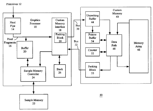
ATI MSAA/ eDRAM module patent for R500/ Xenon?

london-boy said:
I haven't read the whole thread so i apologise in advance if this has been asked and answered before, but isn't the point of eDRAM the fact that it's on the same die, thus allowing much higher speeds and bandwidth than external memory?
If there's an external module, doesn't that defy the whole idea behind eDRAM? Or at least, will it not be much more expensive to get the same performance out of it than it would have if it were on die?
I mean, PS2 has a huge 2048bit bus in the GS because the eDRAM is on the same die. I can't imagine how expensive that would be if it were and external module.

Or am i missing something?

Right.
 
Well, seeing the Xenon diagram again, I'm a bit uncertain now if it's 1 chip or not :? What's this 'Export' at the side of the GPU core :?:
 
one said:
Well, seeing the Xenon diagram again, I'm a bit uncertain now if it's 1 chip or not :? What's this 'Export' at the side of the GPU core :?:

That would also tend to imply a separate north bridge (i.e. its not part of the graphics chip).
 
Looking at that diagram again, it appears that they may have 2 separate busses on the GPU.
1 for incoming data and 1 for outgoing data. That could explain the "Export" block on the diagram.
 
LOL.

There are two busses. But one bus is dedicated to the frame buffer and associated functionality (blending, AA).

You're confusing arrows on that diagram, which are descriptions of data flows, with busses.

The bus between the GPU and Northbridge supports 33.2GB/s. When the GPU writes data to system memory, system memory can only support 22.4GB/s.

A bus does not need to be external between chips to be a bus, either... Although, strictly speaking, it's an interconnect if it only has two nodes, not a bus.

Jawed
 
madmartyau said:
Looking at that diagram again, it appears that they may have 2 separate busses on the GPU.
1 for incoming data and 1 for outgoing data. That could explain the "Export" block on the diagram.

Yeah and it's for exporting to main RAM...Virtual Texturing?
 
When the frame buffer exceeds 1280x720 (if indeed, XBox 360 supports a frame buffer larger than that) it needs to go somewhere...

Presumably all renders to texture will go into system memory.

Jawed
 
Jawed said:
LOL.

There are two busses. But one bus is dedicated to the frame buffer and associated functionality (blending, AA).

You're confusing arrows on that diagram, which are descriptions of data flows, with busses.

The bus between the GPU and Northbridge supports 33.2GB/s. When the GPU writes data to system memory, system memory can only support 22.4GB/s.

A bus does not need to be external between chips to be a bus, either... Although, strictly speaking, it's an interconnect if it only has two nodes, not a bus.

Jawed

I'm not looking at the arrows. Every component has 2 arrows. I'm talking specifically about the "EXPORT" part of the GPU.
 
Tell me which bus or busses you think is/are unidirectional.

How many pins on the GPU is that?...

Jawed
 
"Export" is referring to:

- renders to texture (in main memory)
- completed pixel fragments that need blending/anti-aliasing (in EDRAM)

Jawed
 
Does all this mean that the computations for AA is being done in the edram? Or is this just a silly question.
 
Pugger said:
Does all this mean that the computations for AA is being done in the edram? Or is this just a silly question.

The AA multisamples are generated by the GPU at the same time as the pixel fragments are generated. It seems the GPU is generating 4xAA samples per clock, per pixel.

The pixel fragments and their accompanying AA samples are then sent off for blending and AA. That work is done by a unit that has a dedicated frame buffer memory, with its own private bus. That's the EDRAM.

The EDRAM unit doesn't generate the AA samples, it just manipulates them. It isn't just EDRAM, it's some extra circuitry to do the blending and decide how to use the AA samples.

Jawed
 
what are the chances that the main memory bandwidth - between GPU and Northbridge or GPU and external memory , is higher than 22.4 GB /sec ?

that Xenon Diagram and the Leaked Hardware Overview are probably VERY old. they came out well over a year ago (well the Diagram did) and even then they were already old, probably.
 
Megadrive1988 said:
what are the chances that the main memory bandwidth - between GPU and Northbridge or GPU and external memory , is higher than 22.4 GB /sec ?

that Xenon Diagram and the Leaked Hardware Overview are probably VERY old. they came out well over a year ago (well the Diagram did) and even then they were already old, probably.

I'd guess if the rumoured 512MB system RAM is true, then an increase would be a strong possibility...
 
DaveBaumann said:
one said:
Well, seeing the Xenon diagram again, I'm a bit uncertain now if it's 1 chip or not :? What's this 'Export' at the side of the GPU core :?:

That would also tend to imply a separate north bridge (i.e. its not part of the graphics chip).

and if toyu follow the same logic through the rest of the diagram a seperate video scaler and a seperate AV out chip and .....
 
ERP said:
DaveBaumann said:
one said:
Well, seeing the Xenon diagram again, I'm a bit uncertain now if it's 1 chip or not :? What's this 'Export' at the side of the GPU core :?:

That would also tend to imply a separate north bridge (i.e. its not part of the graphics chip).

and if toyu follow the same logic through the rest of the diagram a seperate video scaler and a seperate AV out chip and .....

It all makes sense now, 'square boxes' means chips...wow! :devilish:

Actually, I thought it was obvious and judging by some reactions here, It was obviously not obvious... <shrugs>
 
>> Why do we get ONLY 48 GB/s on the R500 eDRAM module when we got 48 GB/s on the PS2's GS 5 YEARS AGO?

Could not the eDram module internally have more? The bandwidth requirements between the eDram "module" and GPU should have a fixed max bandwidth requirement of 8 pixels (color and z) per clock x 2 (read + write). No sense in having a bigger pipe there.

In terms of ROP's and ALU performance vs. R420, if the target res is 1280x720 and apps are only increasing in shader length, why does it not make sense to trade ROP's for ALU's. The 6600 showed this nicely. Half of the R420's ALU's are limited instruction set (modifiers, etc.), so 16 full ALU's + 16 mini's. The R500 has 48 complete ALU's with increased precision. There are the same number of texture sampling units in both, though the R500's maybe be better, assuming FP blending, etc. So 48 shader ops (96 if counting vector + scalar or even perhaps vector2 + vector2), and more efficient issuing since the ALU's aren't tied together, plus 16 texture units seems to provide significantly more shading power than R420. Not ignoring the R420's 6 vertex processing ALU's, the R500 still has more raw horsepower and in theory should also be more efficient. It's likely to come up short vs. R520 but in a fixed platform, with a fixed resolution, and bonus eDram for AA, you would imagine it being plenty.

Kinda of off topic, but more than one person has posted about taking steps back to add eDram, SM3.0+, etc. And IMO, the eDRAM module and GPU are seperate.
 
Rockster said:
>> Why do we get ONLY 48 GB/s on the R500 eDRAM module when we got 48 GB/s on the PS2's GS 5 YEARS AGO?

Could not the eDram module internally have more?
Well the leak implies as much, breathlessly stating 256MB/s. But, the techniques here are analogous to Z-data compression, which will give similarly generous "equivalent bandwidth".

Earlier in the thread we briefly touched on the random access bandwidth capability of the EDRAM. The best case appears to be 250MHz for a 90nm EDRAM. How does that translate into the effective bandwidth internal to the EDRAM? Search me.

The bandwidth requirements between the eDram "module" and GPU should have a fixed max bandwidth requirement of 8 pixels (color and z) per clock x 2 (read + write). No sense in having a bigger pipe there.
Absolutely. The leak diagram is fairly specific about this. The GPU sends a stream of finished fragments and lets the EDRAM module do the rest (ROP).

In terms of ROP's and ALU performance vs. R420, if the target res is 1280x720 and apps are only increasing in shader length, why does it not make sense to trade ROP's for ALU's. The 6600 showed this nicely.
Agreed. But R500's ROP is the "EDRAM module". ATI's ahead of you there, lol.

We're still trying to come up with definitive reasons for everything being on one die, or on two. The patent and the leak diagram kinda disagree with each other in terms of grouping functions together (either within the GPU or within the EDRAM).

I prefer to think of both diagrams as logical, only. i.e. neither prescribes physical implementation/locality.

A nice example of this problem is the Sample Memory, 25, in the patent. Oh look, there's a block of memory. Where does it actually reside? On the GPU, a seprate DRAM or as part of the EDRAM?...

b3d16.gif


Jawed
 
Back
Top