AMD: Speculation, Rumors, and Discussion (Archive)

Status
Not open for further replies.
Knowing Nintendo's history, they'd go with a low-end, first-gen GCN GPU hooked to a decade-old CPU core... :p

If they end up with polaris 11, I'll eat my hat. Of course, I don't own any hats, so that'll be an easy one to lose. Either way is good for me - I won't have to eat a hat; Nintendo goes with high-end graphics for first time since N64. Win-win!
 
but using a MOV instruction what kind of latency are you going to incur by doing that. Moving from a register to memory sounds like it will introduce quite a bit waiting period. I can see if it working if its planned for....... by on the fly just doesn't seem likely.
I'm thinking of a move to/from scalar register file from/to vector register file.

I still can't think of a way to do this on the fly. It seems to me it would have to be a bulk move. Some kind of delay seems inevitable, though of course GPUs happily hide latency. Worst case would require moving 256 registers. Somehow I think the amount of state that would be allowed to move would be heavily constrained, e.g. 32 registers.
 
It would need the ability to source an additional operand if FMA were fully implemented. LDS sourcing is another thing the current SALU cannot do, either.
Getting all that into place might make the next step of creating a pipelined FMA unit incremental in complexity. Keeping it as a singular operation would avoid the need to track macro progression in case the GPU opts to preempt things in the next 15 cycles.
The Scalar paper mentioned independent command streams for the scalar.

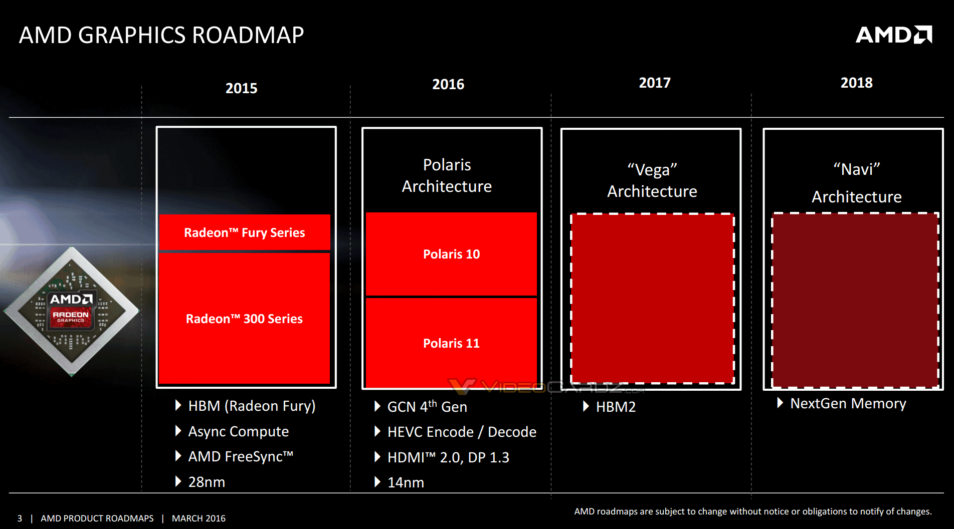
Videocardz has an AMD roadmap showing the Polaris line split evenly between Polaris 10 and Polaris 11.

AMD-Radeon-2016-2017-Polaris-Vega-Navi-Roadmap.png
AMD has mentioned a complete refresh, yet only shown Polaris10/11. That's why I still think we will see a lot of HBM1 and dual die MCMs for higher end parts. They can fab 2 small chips and make their entire lineup. Sure HBM is expensive, but the improved yields from smaller dies will offset some of that and HBM1 is old tech now. It's also smaller than HBM2.

I'm thinking of a move to/from scalar register file from/to vector register file.
What if a per SIMD scalar doesn't have it's own register file and just shares with the VALUs? If the compiler is switching between scalar and vector code paths as needed they shouldn't interfere with each other. Rearranging threads would be a per CU scalar unit which likely would be high performance. That unit could then have a vector sized RF and bulk dump data or update a bunch of indices very quickly. Regrouping an entire thread block would stall a lot of waves without the high performance part.
 
Btw, judging by all the "R9 480(X)($200-250) = R9 390(X)($300-400), both 8GB GDDR5, both at VR-Ready minimum", we could extrapolate and apply that +~30% to virtually every next-gen gpu(AMD and Nvidia), on average it should be +~30%(likely more than less) increase for the same price(!), so, if 480 is around 390, then x60(GP106) should be pretty close as well, making x70(GP104) very close to GM200 cards, with x80(GP104) being at least slightly better than them, and that's just RAW performance, overall, even x70 card should be better choice than 980Ti and TitanX. VRAM-wise x60 should have 4GB GDDR5, x80 - 8GB GDDR5, and 7+1 GB design for x70 seems likely.

So, not +80%-100% like some people expected(largely due to all the hype), but not the "higher performance only for the higher price" as well, +~30% performance for the same price, all things considered, is pretty good.

That's just for anyone who's wondering about how much faster will these cards be and don't want to wait another 2(-6) months, although most people here probably already know...
 
I think the R9 480 family is more probably coming with 4GB GDDR5 under a 256bit bus. That would better fit Tonga's current price level.
Then they can refresh the chip to a R9 580 card with 8GB and raise/maintain its price somewhere in 2017.
Just like they did with Hawaii.

Besides, the VR-Ready moniker points to the R9 290 and the GTX 970, both 4GB cards.
 
Again, long story short, i'd expect ~30% performance-per-dollar increase for all AMD/Nvidia FinFet products coming out soon(direct TitanX successor, however, should be around +50%, even more so for Fury X's), i think that's rather clear now.

I think the R9 480 family is more probably coming with 4GB GDDR5 under a 256bit bus. That would better fit Tonga's current price level.
Then they can refresh the chip to a R9 580 card with 8GB and raise/maintain its price somewhere in 2017.
Just like they did with Hawaii.

Besides, the VR-Ready moniker points to the R9 290 and the GTX 970, both 4GB cards.
Yeah, that possibly could have been the case, especially since full Tonga is not even closed to running out of VRAM(4GB), but they need to differentiate P11 and P10, and there is no way full P11(>R9 370X) is 2gb, even if there is a 4gb option, 2GB just doesn't shine today even for entry level gaming solutions, so while 4gb standart for Non-X 480 is probable, to drive the costs down, 8gb option is likely, and 480X might be 8GB only, like 380X is 4GB only, to further differentiate its line-up.
VRAM amount is one of the biggest AMD's bargaining chips, even bigger today than it was before(go away, Fiji), so, overall, more is likely than less.
 
The compiler knows how to keep the instruction stream valid.
The hypothetical hardware changes explicitly target behavior that AMD claims the compiler cannot determine ahead of time.
If the claim is that static analysis cannot be used to schedule for a dynamic behavior, how is it that it should be able to schedule for the required hazard avoidance of that behavior?

The static analysis doesn't depend on the 4 cycle cadence - it depends on a hardware thread having a constrained set of issues. SALU and VALU are not co-issued from the same hardware thread. The hazards caused by state being in one or the other ALU and required in the following instruction by the other ALU are fully understood.
GCN requires software to paper over hardware gaps in pipeline monitoring and varying paths taken to replace stale data, which is a physical question based on what the hardware is actually doing. Moving what amounts to 32 or 64-bit values in the case of scalar and mask values shouldn't take 20 cycles to "settle". It's a behavior wired into the pipeline and buffers between the independent pipelines that make up the CU, where the hardware does not check and does not update values and assumes the software will fill in the 20 hardware cycles of time it takes to get around to replacing the old data. The problem I see is with one possible embodiment that can drop a statically scheduled 20 cycles to 5 and pull in up to 15 more instructions subject to the stale data if the existing mask handling remains.

Any time some hypothetical new architecture has to decide whether to move state to another ALU, purely for the sake of efficient scheduling, a barrier placed by the compiler will show the hardware where and how it should schedule the move.
The decision making is not up to the compiler in this instance, and would involve a barrier instruction at every block boundary.
The placement of the barrier is also backwards from the memory and export barriers. These are counts based on increment/decrement upon issue/completion of an operation. This scheme needs a barrier that stops when nothing further has been issued yet and the prior instruction is already complete, it would need to be a cycle-counting hang or one that checks pipeline readiness--which would be a check to a pipeline interlock and redundant.

You forget that LDS and global memory operations have variable settling times and there is no consistency problem experienced there. The barriers for these operations are placed there by the compiler too, despite the fact that the compiler doesn't know the settling time.
Those barriers currently exist. The wait states are listed for a portion of GCN where such barriers do not, and where the hardware literally runs blindly into undefined behavior, which I argue means GCN needs to change something in its hardware capabilities or software requirements. However, since it does look like the IP level of Polaris strives to match the prior one in software model, this may rule out any such scheme prior to Vega.

Since these are patents rather than more substantive disclosures, it may also be never.

It would be ironic if the way that execution is switched to a scalar ALU is using a SALU-specific code path generated by the compiler:

Code:
for each x
    if bit_count(exec_mask) > 1 then
        [VALU loop code]
    else
        [SALU loop code]
At least for the patent's scheme, it might not work since the front end scheduler can readily decide to not move a thread to the scalar unit at any given block, regardless of the execution mask. If, for example, a pair of threads on a 2-wide SIMD predicates one thread off while the scalar units are fully subscribed, the active vector thread remains on the SIMD. The claimed benefit was to match wavefronts to physical SIMDs , but a reduced number of wasted lanes was the consolation prize when perfection could not be achieved.
In the other direction, the patent allows for performance counters to prompt the front end to allocate threads to a SIMD with an execution mask in excess of the standard SIMD width and cadence, if it decides other bottlenecks make full ALU utilization counterproductive or unlikely.

The above conditional would need to be replaced with an instruction intended to query what hardware the CU decided to allocate it to. At least the patent appears to keep its allocation decisions at basic block boundaries, otherwise the check would have the potential to fail within a block.

The Scalar paper mentioned independent command streams for the scalar.
The paper posited a more explicit tracking within the program itself, in order to evaluate when utilization was below par.
 
Primitive Discard Accelerator could be big and transparent. Prefetching. ASTC for textures which could be big. Would require some console specific content and repackaging, but not unreasonable. Could also be better color compression for ROPs.
One big BW improvement that people haven't discussed much...

GCN 1.2 texture units are able to directly read lossless compressed GPU resources, such as delta compressed or depth compressed surfaces. This is not limited to reading render targets. You can preprocess (lossless compress) your static textures similarly to save bandwidth on texture reads. Depth compression would be perfect for terrain heightmaps and delta compression would be perfect for most 8, 16 and 32 bit per channel int/float data. Too bad compute shader cannot directly write lossless compressed resources (ROPs only have write capability).

Direct read of lossless compressed data also removes the need to perform costly uncompress operations for color and depth buffers before you can read them.

I would like to know whether delta color compression also supports buffers (linear data). This would make it perfect fit for custom vertex fetch. If not, then you can still store your vertex data to uint32 texture and run it through the ROPs to compress it at startup. Also if fast clear elimination is no longer needed, the fast clear bits could be exploited in funky ways for sparse data structures. Would be fun to play with GCN 1.2 and 1.3.
 
Last edited:
One big BW improvement that people haven't discussed much...
Oh, I mention this all the time ;-).
GCN 1.2 texture units are able to directly read lossless compressed GPU resources, such as delta compressed or depth compressed surfaces. This is not limited to reading render targets. You can preprocess (lossless compress) your static textures similarly to save bandwidth on texture reads. Depth compression would be perfect for terrain heightmaps and delta compression would be perfect for most 8, 16 and 32 bit per channel int/float data. Too bad compute shader cannot directly write lossless compressed resources (ROPs only have write capability).

Direct read of lossless compressed data also removes the need to perform costly uncompress operations for color and depth buffers before you can read them.
Yes indeed, but are you sure about depth compression? I see no evidence the gpu can now do that (I'm just glancing at the open-source driver, which still seems to do a in-place decompress if a depth buffer gets read in the shader).

I would like to know whether delta color compression also supports buffers (linear data). This would make it perfect fit for custom vertex fetch. If not, then you can still store your vertex data to uint32 texture and run it through the ROPs to compress it at startup. Also if fast clear elimination is no longer needed, the fast clear bits could be exploited in funky ways for sparse data structures. Would be fun to play with GCN 1.2 and 1.3.
I don't see anything indicating you could skip decompression for either msaa-compressed surfaces or fast cleared ones. (That said, the allocation of textures, which will also determine the fmask, fastclear, dcc bits disappears somewhere into some address library which I didn't really look at, I don't know if those "old" bits actually still get used for color surfaces...)
 
Polaris only expected to improve perf/watt by 2x, according to Q1 financial results. This is down from 2.5x, isn't it?
http://phx.corporate-ir.net/Externa...yfFBhcmVudElEPTUyMjMwODZ8Q2hpbGRJRD02MzAyNTQ=
"Demonstrated next-generation GPUs
― Polaris architecture-based GPUs are expected to deliver a 2x performance-per-watt improvement over
current generation products and we unveiled upcoming GPU architecture roadmap, including HBM2"
(p. 4)
Sad, if true.
 
Wasn't it always up to 2.5x? I mean perf/W depends on how hard you push it above the sweet spot anyway. So it's not a fixed thing.

Also according to earnings call, Polaris is focusing on mainstream. So below $300 confirmed?
 
Polaris only expected to improve perf/watt by 2x, according to Q1 financial results. This is down from 2.5x, isn't it?
http://phx.corporate-ir.net/Externa...yfFBhcmVudElEPTUyMjMwODZ8Q2hpbGRJRD02MzAyNTQ=
"Demonstrated next-generation GPUs
― Polaris architecture-based GPUs are expected to deliver a 2x performance-per-watt improvement over
current generation products and we unveiled upcoming GPU architecture roadmap, including HBM2"
(p. 4)
Sad, if true.

Perhaps the lawyers said that using Tonga as a basis was good enough for game developers, but not for the people that can sue you.
 
Too bad compute shader cannot directly write lossless compressed resources (ROPs only have write capability).
I'd still wonder about cached writes for compute that may allow this. With all the recent compute based postprocessing I can't imagine it's not work looking into. I've seen absolutely nothing on this capability, but it would help.

Direct read of lossless compressed data also removes the need to perform costly uncompress operations for color and depth buffers before you can read them.
This I didn't realize was getting added. That was one of the huge sticking points with Tonga/Fiji as I recall.

I see no evidence the gpu can now do that (I'm just glancing at the open-source driver, which still seems to do a in-place decompress if a depth buffer gets read in the shader).
That was a big gotcha they were pointing out at GDC. Maybe behavior has changed, but as of this past year it was still tripping up developers.

How much of a perf/watt increase is attributed to the new process?
I thought FINFET was 20-35% perf or 60% less power. So at lowest possible clocks they'd have the 2.5x. This could just mean they decided to increase clocks a bit for competitive reasons. Still seems pretty conservative, and I'm sure they could go lower.
 
-60% power only if you stay at 28nm level transistor sizes - not when you intend to shrink the chip as well for the sake of production cost.

It's the shrinking of the transistors that saves power. Think about it in terms of smaller transistors need less energy to switch. You can get back to similar power levels as the previous node by adding more transistors (for more performance) or faster switching (higher clock speeds).
 
I have not seen any requirement that the FinFET process can only significantly reduce power by not shrinking transistor features at all from 28nm. I am not sure that is even offered by the processes as an option. Playing with transistor size in that manner is more readily done for planar devices, whereas fin count is used in place of sizing for FinFET.

The Tesla P100 increases TDP by 17% with a 90% increase in transistor count, on a device that upclocks by nearly 400MHz relative to its Maxwell predecessor.
 
I believe fin height can also be used for increasing performance with FinFETs and is probably the difference between the early 14/16nm and the current LPP/FF+ available now.
 
Status
Not open for further replies.
Back
Top