Install the app
How to install the app on iOS
Follow along with the video below to see how to install our site as a web app on your home screen.
Note: This feature may not be available in some browsers.
You are using an out of date browser. It may not display this or other websites correctly.
You should upgrade or use an alternative browser.
You should upgrade or use an alternative browser.
AMD: Speculation, Rumors, and Discussion (Archive)
- Thread starter iMacmatician
- Start date
- Status
- Not open for further replies.
D
Deleted member 2197
Guest
Sapphire Nitro+ RX 480 4GB Review
http://www.overclockersclub.com/reviews/sapphire_nitro_rx_480_4gb/
Review: MSI Radeon RX 480 GAMING X
http://www.guru3d.com/articles-pages/msi-radeon-rx-480-gaming-x-review,1.html
http://www.overclockersclub.com/reviews/sapphire_nitro_rx_480_4gb/
Review: MSI Radeon RX 480 GAMING X
http://www.guru3d.com/articles-pages/msi-radeon-rx-480-gaming-x-review,1.html
Last edited by a moderator:
Alessio1989
Regular
Here's another video showing how easy is to clean the Nitro+ fans
ImSpartacus
Regular
I saw this Anandtech article on SK Hynix's Q3 lineup including 4GB HBM stacks at 1.6 Gbps & 2 Gbps. What's the consensus for HBM configurations on Vega? Is it generally assumed that both little and big Vega will both use HBM? I've been out of the rumor mill loop.
My gut says that a GP104-competing little Vega would use two stacks of 4GB HBM at roughly 1.6 Gbps. That would yield the same VRAM capacity as GP104 and roughly 25% more bandwidth. AMD GPUs tend to have slightly more bandwidth than equivalent competing Nvidia GPUs, so I think that ratio seems reasonable.
But what about big Vega? If it competes with GP102, then it oughta be roughly 1.5x of GP104-competing little Vega since GP102 is roughly 1.5x of GP104. If little Vega would use two stacks of 4GB HBM, then big Vega oughta use three stacks, right?
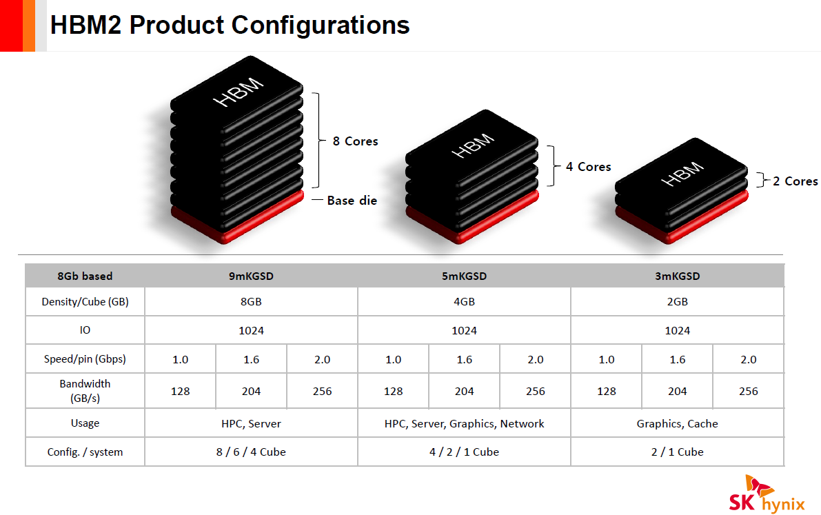
However, is a 3-stack configuration even possible? I noticed that an old SK Hynix slide only lists "4 / 2 / 1 Cube" for "Config. / System". Is that the possible number of stacks for a given system?

It would kinda suck if big Vega was forced to use a full-blown 4-stack configuration. In that case, I imagine it would be underclocked similar to the P100.
Also, what HBM parts is Samsung making? I recall an old article stating that they are in mass production, but I didn't see anything in their catalog. I'm assuming someone has to be producing the HBM for GP100-based stuff.
My gut says that a GP104-competing little Vega would use two stacks of 4GB HBM at roughly 1.6 Gbps. That would yield the same VRAM capacity as GP104 and roughly 25% more bandwidth. AMD GPUs tend to have slightly more bandwidth than equivalent competing Nvidia GPUs, so I think that ratio seems reasonable.
But what about big Vega? If it competes with GP102, then it oughta be roughly 1.5x of GP104-competing little Vega since GP102 is roughly 1.5x of GP104. If little Vega would use two stacks of 4GB HBM, then big Vega oughta use three stacks, right?
However, is a 3-stack configuration even possible? I noticed that an old SK Hynix slide only lists "4 / 2 / 1 Cube" for "Config. / System". Is that the possible number of stacks for a given system?

It would kinda suck if big Vega was forced to use a full-blown 4-stack configuration. In that case, I imagine it would be underclocked similar to the P100.
Also, what HBM parts is Samsung making? I recall an old article stating that they are in mass production, but I didn't see anything in their catalog. I'm assuming someone has to be producing the HBM for GP100-based stuff.
Big Vega will presumably be targeting the top of the professional market (to replace the more than 2 year old W9100, it will have to compete with both GP100 and GP102), which will pay a lot of money for as much memory as possible. Thus 4-stacks makes sense. As with GP100, we might see cut-down 3-stack SKUs.
Price were discus on Polaris launch. 150 / 100
I think they mentioned that they want to target those price ranges but they didn't give any hard pricing did they?
$150 seems too low for a part which should offer between 85-90% of RX480's performance.
Big Vega will presumably be targeting the top of the professional market (to replace the more than 2 year old W9100, it will have to compete with both GP100 and GP102), which will pay a lot of money for as much memory as possible. Thus 4-stacks makes sense. As with GP100, we might see cut-down 3-stack SKUs.
Yep agreed. I'm not so sure little Vega needs HBM though, GDDR5X at 11-12 Gbps (I'm assuming these will be available by Q4'16 or Q1'17) on a 256 bit bus ought to be sufficient (With 64 ROPs though)
GDDRX5 would mean that AMD would have to invest into their GDDR memory controller, which is still less effective than Nvidia's version. I think Vega will be HMB with the little one using 2x4GB stacks, the big one probably four. With the option of going to 32GB.
"Less effective" in what way? They've already laid the groundwork with 8 Gbps on Polaris. The higher price of HBM for a consumer card is not really justified.
Alessio1989
Regular
Here's another video showing how easy is to clean the Nitro+ fans
While our Rx 480 Nitro+ review is still not available, yesterday we received also the 460 Nitro. ( :
Less effective because a similar memory OC on a 1070 and a RX480 gives you similar performance gains, while the overall performance and processing power is not similar."Less effective" in what way? They've already laid the groundwork with 8 Gbps on Polaris. The higher price of HBM for a consumer card is not really justified.
I personally hope for HBM on Desktop Vega, that would significantly improve browser, multi-monitor and video decode power consumption. Since AMD hasn't yet managed to built to a GDDR5 memory controller in the past eight years with adequate clocking support (one that doesn't switch to full-speed clocks if you move the cursor) HBM is my only hope on that front.
But that is not only matter of memory controllers.Less effective because a similar memory OC on a 1070 and a RX480 gives you similar performance gains, while the overall performance and processing power is not similar.
CaptainGinger
Newcomer
I personally hope for HBM on Desktop Vega, that would significantly improve browser, multi-monitor and video decode power consumption. Since AMD hasn't yet managed to built to a GDDR5 memory controller in the past eight years with adequate clocking support (one that doesn't switch to full-speed clocks if you move the cursor) HBM is my only hope on that front.
I couldn't agree more, the way AMD handles memory clocks in these low power situations seems like it's from the dark ages.
I think they mentioned that they want to target those price ranges but they didn't give any hard pricing did they?
$150 seems too low for a part which should offer between 85-90% of RX480's performance.
Well thats the official price, if partners are going to sell it more expensive IDK.
An update: The Sapphire are back in the listing in Amazon but still no stock. Btw will any website list the nitro in its official price of 210? cuz everything I've seem is 230.
Granted, I personally think the color compression is less effective at AMD, but even working on this is an extra effort when you could go for HBM with lots of additional bandwith.But that is not only matter of memory controllers.
New RSCE 16.7.3/16.8.1 can do more than 10% perf improvement for RX 480, comes only out when paired with lower end CPUs.
http://www.pcgameshardware.de/AMD-R...euer-Treiber-Rise-of-the-Tomb-Raider-1203196/
Up to 20% in real gameplay(tm)
http://www.pcgameshardware.de/AMD-R...euer-Treiber-Rise-of-the-Tomb-Raider-1203196/
Up to 20% in real gameplay(tm)
D
Deleted member 2197
Guest
Review: MSI Radeon RX 470 Gaming X 8GB
http://www.guru3d.com/articles-pages/msi-radeon-rx-470-gaming-x-8gb-review,1.html
Edit:
Review: PowerColor Radeon RX 470 RED Devil 4GB
http://www.guru3d.com/articles-pages/amd-radeon-rx-470-4gb-review-powercolor,1.html
Review: ASUS Radeon RX 470 STRIX Gaming 4GB
http://www.guru3d.com/articles-pages/asus-radeon-rx-470-strix-gaming-4gb-review,1.html
Last edited by a moderator:
Sapphire Nitro RX 470 OC
Keeps it at 130 Watts
http://www.59hardware.net/articles/cartes-graphiques/sapphire-nitro-rx-470-oc-2016080418128/9.html
Keeps it at 130 Watts
http://www.59hardware.net/articles/cartes-graphiques/sapphire-nitro-rx-470-oc-2016080418128/9.html
Last edited:
GPU Power Draw. That's the 110 Watt of the RX 480 you read before launch. Just sayin.Sapphire Nitro RX 470 OC
Keeps it at 130 Watts
http://www.59hardware.net/articles/cartes-graphiques/sapphire-nitro-rx-470-oc-2016080418128/9.html
Realistically, the cards consume between 140 and 150 watts (our Asus Strix O4G has a power limit of 146 watt).
- Status
- Not open for further replies.
Similar threads
- Replies
- 90
- Views
- 18K
- Replies
- 2K
- Views
- 238K
- Replies
- 20
- Views
- 7K
