AMD RyZen CPU Architecture for 2017

I dont know why you guys get hung up on this stuff, unless something is drastically wrong with a very large portion of those good 8 core dies you are only taking a few dollars remember there are near 300 chips a wafer. if we assume stupid numbers.

wafer cost 7k
80% yield 20 % failure (237 dies) = $29
70% yield 30% failure (207 dies) = $33
60% yield 40% failure (178 dies) = $39

Now if 80% of dies have all 8 core and are functional how many of the SOC with failures are still usable, it could still easily be 50% of those, so 90% that "work" as a CPU. So the lowest bin is 3.2/3.4ghz, now if we look at something like 1600/1700 vs 1800x the extra binning is only buying you on OC about 200mhz so do we really think there are these hordes of dies that can't reach 4 core 3.2/3.4 in 65watts?

Personally i would find that a little odd.....
So if they can all reach a minimum of 4c 3.2/3.4 thats $23 a die,
90% of 90% (240 dies) = $29
80% of 90%(213 dies) = $32

Then think about this, amd could take all these rubbish clocking dies ( if they actual exists) put them on an MCM and sell them as a Xeon-D competitors 16/24/32 core ~2ghz clock 45-95watt.

Really we are talking about $10 a chip here, if we assume revenue per cpu averages out at $219MSRP (1600, 3rd lowest of 7 sku's) your talking 4.5% of its cost 10million dollar on 219 million of MSRP revenue. its not making or breaking anything.

i'll also add that well over a year ago Samsung said 14nm LPP had 0.1 sq cm defect density ( 80% 0 defect yield on 200mm sq)............
 
I dont know why you guys get hung up on this stuff, unless something is drastically wrong with a very large portion of those good 8 core dies you are only taking a few dollars remember there are near 300 chips a wafer. if we assume stupid numbers.
My main point is not to read too much into a fragment of a leak. It's worded in a way that is ambiguous, and there are some significantly different interpretations to the statement because it omits a lot of the context. Saying it in that fashion may be purposefully leading the reader to take certain leaps.

Now if 80% of dies have all 8 core and are functional how many of the SOC with failures are still usable, it could still easily be 50% of those, so 90% that "work" as a CPU.
The statement is simply that 80% of dies have 8 functional cores, which I am interpreting at a minimum to mean the cores and their dedicated resources are able to run correctly. This includes core logic, the hooks into the CCX, and the per-core L2.
In this scenario, irrecoverable defect rate is the determining factor and not how readily 8 functioning cores can fit within the specs of any given SKU.

One unknown is that the CCX and core section has areas of rather low defect tolerance like the internal core units (complex, tightly packed, higher performance devices, little redundancy etc.) and others with significant recovery options like SRAM (regular structure, spare rows, etc).
How the rest of the SOC compares is unclear (lower speeds, more area, components physically sized for IO--meaning more tolerance for variation, unknown redundancy, etc.).

Per the leak, a Zeppelin die has something like 56mm2 of core functional area, and 20% of the time it has at least one irrecoverable defect. A decent chunk of that area is cache or some other form of SRAM, which should be far more capable of recovery against defect. It could be something like 36-40mm2 total if we assume some recovery options there reduce fatal defects to low levels in those regions.

It's a better number if "functional" means the determination is made after all other reasons for deactivating a core to meet performance and power parameters have been satisfied. It can be better if this is arrived at after other fault sources are taken into account. That's a generous reading of the sparse statement, however.

i'll also add that well over a year ago Samsung said 14nm LPP had 0.1 sq cm defect density ( 80% 0 defect yield on 200mm sq)............
That's also Samsung and not GF. The latter was over a year behind a year ago, and is still struggling to distinguish itself positively in terms of execution.
What type of chip was being used as the basis, its yield recovery measures, and parameters for the silicon have little public data to compare with Zeppelin's mostly undisclosed methods and parameters.

In terms of chips with less than 8 functional cores, a more optimistic assumption is to give 56mm2 to core area out of 200-220mm2.
.56cm2 with a rate of at least one uncrecoverable defect 20% of the time is at least .36 defects per cm2 in that component, so I think there's something not comparable between the two low-context values. It would be worse if the SRAM is assumed to drop to a minor contribution, as much of the chip is not obviously made of cache and that would mean the arrays are hiding a higher background rate of recovered faults.
What level of fault tolerance, physical resistance to failure, or recovery is built into the rest of Zeppelin is not part of the leak. Hopefully the irrecoverable fault rate is lower for the ~120mm2 of the chip that is not core or L3. Depending on the relative resilience of the regions, it could increase the chance of losing units outside of the core at several times the rate of having fewer than 8 cores. There aren't any SKUs that have lost their PCIe controller, or blew out a chunk of their data fabric, for example.
 
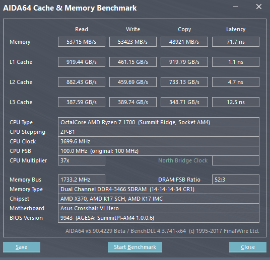
Currently testing AGESA 1.0.0.6 on the C6H (spoiler: It's really good :))

4nou1w.png
 
It gives you access to 2T and a lot more, I've just started messing with the sub-timings and there's just so much there :)
 
Well I've got 3466CL14 pretty much 99.9% stable at 1.4v:

ramzou4x.png


Lowered some sub-timings and raised others to get to that, AMD has set weird settings at stock for the memory timings, that's for sure. AGESA 1.0.0.6 also provides access to memory multipliers for 3466/3600/3733/3866/4000 MT/s without any bclk overclocking.
 
I don't want a lot, but my 3200 ram working higher than 2400 would be nice :)
Same here, I am stuck at 2666MHz when the mobo max and RAM modules max is 3200. MSI hasn't updated the bios file of the BM350 yet
 
Same here, I am stuck at 2666MHz when the mobo max and RAM modules max is 3200. MSI hasn't updated the bios file of the BM350 yet
We're probably a couple of weeks away at least from these BIOS updates being released.
 
It gives you access to 2T and a lot more, I've just started messing with the sub-timings and there's just so much there :)

The Stilt made some interesting measures how much timings actually effect gaming. Quite huge difference actually.

3200MHz results are with CL16-16-16 timings, and 3200 LL are with CL12-12-12 with additional subtimings tightened.

KxdrYPc.png

Original post (in finnish) https://bbs.io-tech.fi/threads/amd-ryzen-7-am4-b350-x370-kellotukset-ja-kokemukset.14849/page-51
 
So from totally playable to totally playable?
Really? Because no one plays on high refresh monitors, or wants to push AA or details more, or many other reasons we like to tweak things on PC to get the best that our hardware can do. Let's just sell all our GPUs and buy consoles. Sorry, what forum section are we in?
 
Back
Top