To be honest I read emulation of fixed function units more like emulating ROPs, presumably accelerating rendering in higher resolutions, while using less die space. Don't know why my mind thought of that, probably because tensor cores are anything but fixed function.There's nothing to 'emulate' in tensor/xmx/matrix cores, they're just accelerating normal matrix math. As for precision, RDNA2 goes all the way down to 8:1 INT4 so yeah, you can pick lower precisions for inferencing if you want.
Install the app
How to install the app on iOS
Follow along with the video below to see how to install our site as a web app on your home screen.
Note: This feature may not be available in some browsers.
You are using an out of date browser. It may not display this or other websites correctly.
You should upgrade or use an alternative browser.
You should upgrade or use an alternative browser.
- Status
- Not open for further replies.
davis.anthony
Veteran
That's how I read it to, when the GPU is front/back end limited it emulates these units to try and boost performance.To be honest I read emulation of fixed function units more like emulating ROPs
Last edited:
Keep any rumors and speculations before hand in this thread.
During and after the reveal the new discussion thread to use is here:

 forum.beyond3d.com
During and after the reveal the new discussion thread to use is here:
AMD RDNA3 Specifications Discussion Thread
Start of a new technical thread for AMD RDNA3 specifications once they are revealed. The rumor thread leading up to the event: https://forum.beyond3d.com/threads/amd-rdna-3-speculation-rumours-and-discussion.62092/
forum.beyond3d.com
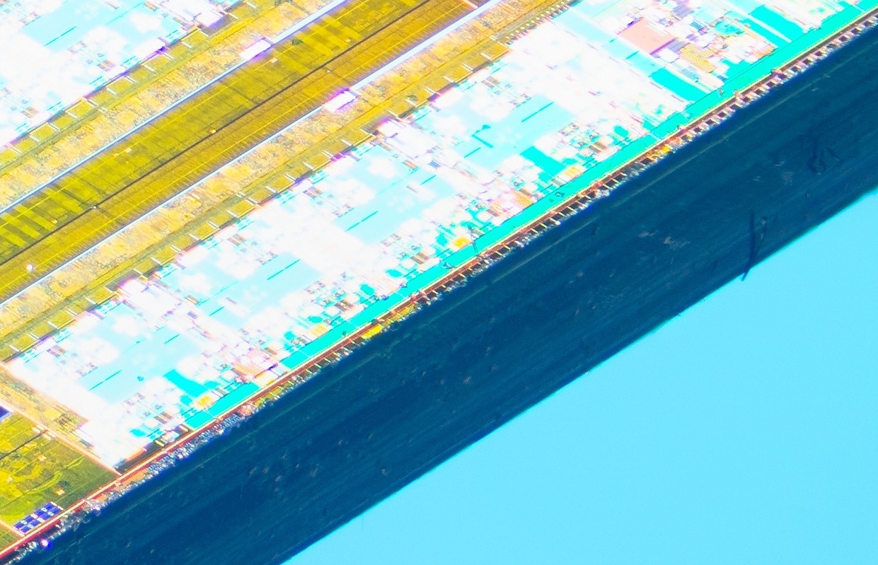
I agree with your first set of numbers for GCD and MCD (they are very close to the ones Angstronomics told us a while ago [305mm² and 37.5mm², respectively]). But what is the "molding overhead" supposed to be? The visible edges of the dies in the mold are the real edges of the dies as cut from the wafer.
Quick and dirty die areas derived from the low-resolution Angstronomics picture.
Jawed
Legend
Discussion starts here:I agree with your first set of numbers for GCD and MCD (they are very close to the ones Angstronomics told us a while ago [305mm² and 37.5mm², respectively]). But what is the "molding overhead" supposed to be? The visible edges of the dies in the mold are the real edges of the dies as cut from the wafer.
ELSA hints GT206 and GT212
... GT200 isn't nearly bandwidth starved even with GDDR3 ... If you own a GTX 280, i can provide a sample where the frame rate is almost linear with the bandwidth of the card. I'm waiting for a 512bit GDDR5 monster. That day, i'll say 'goodbye' to my performance problems.
forum.beyond3d.com
with Dave Baumann providing an official comment, demonstrating that (not for the first time) measurements of a packaged die are always too large. 0.5mm is just an approximate correction...
Of course I could re-do my die-size estimates based on the dimensions stated by the website (308 and 37.5mm²) with a correction of the linear dimensions by 0.5mm: e.g. 289.7mm² and 31.6mm²; we'll get much better numbers at some point
")
Henry swagger
Newcomer
Guess the rumours are true 7900 xtx is 45% better than the 6900xt.. doubling cores ampere like is not scaling well ? 
davis.anthony
Veteran
Guess the rumours are true 7900 xtx is 45% better than the 6900xt.. doubling cores ampere like is not scaling well ?
I imagine the poor scaling is also the result of current games and engines, they're not pushing the GPU's hard enough to get good scaling with wider GPU's.
I do expect them to get better as games start to use DX12U more.
Radeon RX 7900 XTX runs at ~50 % higher clock than Radeon RX 6900 XT, and it has >50 % higher raw bandwidth. Even Radeon RX 6900 XT GPU running at these clocks and having this bandwidth would be more than 45 % faster.Guess the rumours are true 7900 xtx is 45% better than the 6900xt.. doubling cores ampere like is not scaling well ?
Discussion starts here:
ELSA hints GT206 and GT212
... GT200 isn't nearly bandwidth starved even with GDDR3 ... If you own a GTX 280, i can provide a sample where the frame rate is almost linear with the bandwidth of the card. I'm waiting for a 512bit GDDR5 monster. That day, i'll say 'goodbye' to my performance problems.
with Dave Baumann providing an official comment, demonstrating that (not for the first time) measurements of a packaged die are always too large. 0.5mm is just an approximate correction...
Of course I could re-do my die-size estimates based on the dimensions stated by the website (308 and 37.5mm²) with a correction of the linear dimensions by 0.5mm: e.g. 289.7mm² and 31.6mm²; we'll get much better numbers at some point
Dave's comment alluded to the "official" size (scare quotes are in the original) of a specific chip (RV740), probably as designed, before taking the extra space needed for dicing into account and in my opinion doesn't really relate to your 0.5mm here.
The comparison was with a obviously quite rough measurement of some guy at hexus.net, who only said (rounded?) 12mmx15mm for the die dimensions. "Official" was 170mm² according to Dave. That could have been 11.62mm x 14.63mm for all we know. Then add let's say 50µm for the (dicing strait - scribe line width)* and we would have ended up with 11.67mm x 14.68mm as the actual physical die with a careful measurement.
Or maybe the difference between the "pre-silicon number" and the "final 'official' size" is the area required for the dicing? That would be pretty much exactly 0.15mm (150µm) in this case (from 2009). Hey, that fits pretty well with my number below I wrote before adding this spoiler!
*: depending on how the dicing is actually done, the subtraction may not be warranted as the wafer may not be cut through completely. In that case one can usually see a small step on the side of the dies (not for N31 of course, because of the mold).
0.5mm is way too much for the necessary dicing strait/scribe line width between dies. More common should be 100µm or maybe slightly more, but definitely below 0.2mm (and a part of that is removed during dicing, so would not be included in the photo). In the end, who cares about how much less space the design takes from the outer dimensions of the die? AMD, intel, and nV do, for sure, but not we. They have to pay for the whole area of the wafer (including the space needed for dicing). If some company wants to leave 1mm space between dies, TSMC will let them do that, but that would be quite a waste of money.
Anyway, my point was that one actually sees the actual edges of the physical die in that photo. And that are the important dimensions (especially for the costs). That's why you should simply stick to your first set of number (~303mm² and 36mm²) and not apply some (misguided) "corrections". Your "uncorrected" numbers are probably closer to the correct ones (assuming the given package dimensions are correct).
Last edited:
digitalwanderer
Legend
Would y'all believe I'm actually a bit more interested in performance-per-dollar in how AMD and nVidia compare this round? I think they'll both have beastly GPUs, I'm just hoping they're not all insanely priced. I think I'm most looking forward to hearing about the 7000 series MSRP.
Jawed
Legend
0.5mm may be a rule of thumb if one does a very crappy measurement with a caliper and measures not just the die but includes some underfill "leaking" out of the sides of the die in the measurement.Dave's comment alluded to the "official" size (scare quotes are in the original) of a specific chip (RV740), probably as designed, before taking the extra space needed for dicing into account and in my opinion doesn't really relate to your 0.5mm here.
The comparison was with a obviously quite rough measurement of some guy at hexus.net, who only said (rounded?) 12mmx15mm for the die dimensions. "Official" was 170mm² according to Dave. That could have been 11.62mm x 14.63mm for all we know. Then add let's say 50µm for the (dicing strait - scribe line width)* and we would have ended up with 11.67mm x 14.68mm as the actual physical die with a careful measurement.
Or maybe the difference between the "pre-silicon number" and the "final 'official' size" is the area required for the dicing? That would be pretty much exactly 0.15mm (150µm) in this case (from 2009). Hey, that fits pretty well with my number below I wrote before adding this spoiler!
*: depending on how the dicing is actually done, the subtraction may not be warranted as the wafer may not be cut through completely. In that case one can usually see a small step on the side of the dies.
0.5mm is way too much for the necessary dicing strait/scribe line width between dies. More common should be 100µm or maybe slightly more, but definitely below 0.2mm (and a part of that is removed during dicing, so would not be included in the photo). In the end, who cares about how much less space the design takes from the outer dimensions of the die? AMD, intel, and nV do, for sure, but not we. They have to pay for the whole area of the wafer (including the space needed for dicing). If some company wants to leave 1mm space between dies, TSMC will let them do that, but that would be quite a waste of money.
Anyway, my point was that one actually sees the actual edges of the physical die in that photo. And that are the important dimensions (especially for the costs).
The issue is that the smaller the die area, the larger the impact the measurement error has upon the die area. The error, whatever it turns out to be for the small die, is looking to be quite substantial...
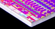
Also, when looking at die shots such as:
Fritzchens Fritz’s albums | Flickr
 www.flickr.com
you'll usually see that there is, indeed, a non-functional perimeter to dies - and that's after sawing. When talking about costs or performance per unit area there's just a bit more error because of that - but costs should be based upon wafer layout for the chips (and yields).
There could be 300+ chips difference for a 12" wafer for this small die according to:

Die Per Wafer (free) Calculator - Trusted by Amkor and GF
How can you calculate the number of dies per wafer? A free online tool, DPW equation and reference to two other DPW calculators. Trusted by Amkor and GF.
based upon 7.4x5.1 versus 6.9x4.6mm (adjusted by me from the Angstronomics numbers - not those derived and adjusted by me from the picture) = 1636 versus 1949...
I expect the real dimensions to be somewhere between my low estimate and the approximate Angstronomics numbers - originally they come with a "~"
Actually, if you look at the pictures with the right lighting, one can see there is almost no space left at all.The issue is that the smaller the die area, the larger the impact the measurement error has upon the die area. The error, whatever it turns out to be for the small die, is looking to be quite substantial...
Also, when looking at die shots such as:
Fritzchens Fritz’s albums | Flickr
you'll usually see that there is, indeed, a non-functional perimeter to dies - and that's after sawing. When talking about costs or performance per unit area there's just a bit more error because of that - but costs should be based upon wafer layout for the chips (and yields).
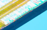
How thick is a typical wafer? Depending on what you do, it is often about 0.7mm, isn't it? That means there is less than 100µm (50µm?) space from the edge of the die in the following pictures.
That's a 7nm design from AMD (PS5):
And this a 16nm AMD chip (XB1-S):

Here you can also nicely see the the small edge on the side of the die caused by the different dicing method I mentioned earlier.
The dicing area is sometimes used for test structures for wafer leving testing (they get partially destroyed by dicing). But in these photos the functional structures of the chip extend extremely close to the actual edge of the die.
That's a 7nm design from AMD (PS5):
And this a 16nm AMD chip (XB1-S):
Here you can also nicely see the the small edge on the side of the die caused by the different dicing method I mentioned earlier.
The dicing area is sometimes used for test structures for wafer leving testing (they get partially destroyed by dicing). But in these photos the functional structures of the chip extend extremely close to the actual edge of the die.
Last edited:
Added street markings, rough yellow and red lines. I wasn't super precise but you can make out the streets due to the pads.Actually, if you look at the pictures with the right lighting, one can see there is almost no space left at all.
How thick is a typical wafer? Depending on what you do, it is often about 0.7mm, isn't it? That means there is less than 100µm (50µm?) space from the edge of the die in the following pictures.
That's a 7nm design from AMD (PS5):
And this a 16nm AMD chip (XB1-S):
Here you can also nicely see the the small edge on the side of the die caused by the different dicing method I mentioned earlier.
The dicing area is sometimes used for test structures for wafer leving testing (they get partially destroyed by dicing). But in these photos the functional structures of the chip extend extremely close to the actual edge of the die.
Edit- I'm not sure how big streets are on modern processes/wafers. I mostly dealt with +130nm 8in wafers down to maybe 40nm 12in wafers (might have gone down to 28nm, not sure).
Attachments
Jawed
Legend
This video focuses on how TSMC plans to get past 3nm. A major problem with the coming generations of process technology is that multi-patterning will have to be used for more layers. Multi-patterning slows down the machine, reducing the count of wafers per hour it can produce.
The need for multi-patterning can be reduced by increasing the magnification of the optical system which goes hand in hand with increasing the numerical aperture. The side-effect of the increased magnification is that the reticle area is reduced!
One aspect of the solution is a revised optical system that uses anamorphic projection.
The end result of all this pain (about a decade of pain, it seems) is that you end up with a reticle that's only 16.5x26mm. This appears to imply that the largest conventional chip produced by this process is 429mm².
So it turns out that chiplets are needed simply to avoid crashing into this area limitation. But this problem only becomes real in 2025 or later, it seems? So RDNA 5?...
Bondrewd
Veteran
hNA has been pushed waaaaaaaaay up, think 2027+ timeline for prod steppers.But this problem only becomes real in 2025 or later, it seems?
Just don't think about it for now, really, it's still in voodoo magick stage.
But yes, reticle will be cut in half so vewy complex MCPs are very much the only future left for us all.
- Status
- Not open for further replies.
Similar threads
- Replies
- 1K
- Views
- 187K
- Replies
- 15
- Views
- 2K
- Replies
- 7
- Views
- 3K
- Replies
- 85
- Views
- 12K