AMD: R9xx Speculation

Some hints about the RV970 ?

Hundred hands... maybe they want people to assume they are staying with their current shader setup, since every hand has 5 fingers?
1 SP = 5 ALU, 4 "regular" and 1 "fat".
1 hand = 5 digits, 4 "fingers" and 1 "thumb".

;)


Lucid HYDRA 200 Details With AMD, Lucid & NVIDIA
Legit Reviews: Lucid recently said that GPU frame rendering methods that are being used by both ATI and NVIDIA were primitive and that you are limited by AFR [Alternate Frame Rendering] and SFR [Split Frame Rendering]. Is this true?

AMD: If there are new multi-GPU problems that we want to address, AMD is more than capable of developing the right technique for the problem. In fact, you will hear more of this in the near future.

Legit Reviews: When it comes to multi-GPU systems ATI allows you to run CrossFireX on identical series of cards no matter who the manufacturer is and you allow users that want to run CrossFire to mix and match different cards within a particular series. Is there a reason that you only allow mixed CrossFire to work in a particular series?

AMD: ATI is committed to delivering a great gamer experience with CrossfireX. Mixing cards from different series can lead to game compatibility problems, often eclipsing performance benefits. That being said, there are a whole host of CrossfireX innovations that we have in the oven. All in good time.
 
Somehow i disbelieve R900 is brand new architecture, just lightweight pure VLIW on R600 heritage w/o unnecessary things like RBEs and TMUs maybe with DX12 compliance.

DX12 will not come for many years. Next-generation radeon chips will come in next year.

And "new dx version complicity" is not just some feature you bolt into existing design, it usually requires complete redesign of the architecture, ATI's DX10->DX11 was about the only exception to this (and it was mostly because ATI's DX10 generation already almost supported the new features (ie had the features, but with implementation which was not compatible with the DX11, so AMD just had to update them to DX11 level/make them compatible with the DX11 specifications)

Even though R870 performs well, it's starting to show it's 2.5 year age.

So just an dx11 refresh guess drops out here. And it will be all that R800 with DX11 compliance didn't need to be.

This is the logic (and words) which I don't understand.

Probably 256-bit wide SIMD units with 2x 32b wide SFUs for transcendentals (instead just one in R600 based cores).

It's already 512-bit(16*32) wide SIMD ( * 5 -way VLIW ), ie total width of 2560 bits.

2-way SIMD(*16) transcendentals would not make much sense, there would not be much code that would take advantage of it.

But if you mean 8-way SIMD / pixel, (or "software thread") , would not make sense as widest vectors that are calculated per pixel or per vertex are usually 4-wide, and the more advanced shaders we have, the more we have scalar calculations.

ATi already changed from SIMD to VLIW on this level, because even those 4-way vectors are so rare with more advanced shaders, that VLIW gives much better performance.. and even the VLIW cannot often be utilized very well.

Or maybe fully armed 512bit wide SIMDs:LOL: Meh, that's overkill imho and certainly not a way to go.

No, it's what they have now.

But if you mean 512-bit wide sim / one software thread.. would make absolutely no sense.

So while we still have only 20 cores x16SIMDs x5SP, then we could have 32SIMD x8SP per core and let's say 32 cores (extra 8 cores included to substitute missing ROP functionality) = 8192SPs.

... And most of those ALU's (IMHO the correct word instead of new fancy words like SPU) idling most of the time because the compiler cannot find anything for them to do, when the instruction stream just does not have enough instruction-level parallelism.

We already see this when we compare RV770 to GT200; RV770 has about double the theoretical flops of GT200 but it's slower in practice.

Anand's RV870 review has nice example image of this:

http://www.anandtech.com/video/showdoc.aspx?i=3643&p=4


And do you want to get rid of the ROP's/RBE's? And replace those with software?

I don't know where they'll fit it but considering RBEs & TMUs waste 40% of die space in RV770 and with triple packed SPs per core i guess they could fit it pretty nice under 300mm2 @28nm and with 1.2-1.5GHz clock rate. Especially if we make assumption that inventive 28nm will have extremely reduced leakage considering even 32nm shrink claims almost 40% less leakage than 45nm TSMCs process

Leakage problems typically increase when going to smaller process. With some processes we are getting better because some new technologies have been adopted to combat leakage, but there are not endless pockets of those technologies, and if we do just "simple process shrink" we get worse leakage.
 
Last edited by a moderator:
... And most of those ALU's (IMHO the correct word instead of new fancy words like SPU) idling most of the time because the compiler cannot find anything for them to do, when the instruction stream just does not have enough instruction-level parallelism.

We already see this when we compare RV770 to GT200; RV770 has about double the theoretical flops of GT200 but it's slower in practice.

Anand's RV870 review has nice example image of this:

http://www.anandtech.com/video/showdoc.aspx?i=3643&p=4
Utilisation on VLIW in games is fine:

http://forum.beyond3d.com/showthread.php?p=1220350#post1220350

Anandtech is clueless on this subject.

Jawed
 
Utilisation on VLIW in games is fine:

http://forum.beyond3d.com/showthread.php?p=1220350#post1220350

Anandtech is clueless on this subject.
Still room for improvement, though, as we recently learned from NVidia that GT200 can't issue transcendentals and MADs simultaneously, so that would give a proper scalar design a decent boost. I wouldn't be surprised if ATI's utilization was 60% on average rather than the 75% one gets from your data when incorrectly assuming the GTX280 has 100% utilization.

But don't be too hard on Anandtech, as they're just giving an example to illustrate the difference, even if it is a bit atypical.

hkultala, you are making a huge blunder in assuming that the graphics loads are mostly limited by shader math. Remember that the GT200 has twice the ROPs of RV770, twice the TMUs, and twice the bus width. Yes, lower clocks reduce those advantages a bit, but they're still very substantial, and they paid for all this with a huge piece of silicon. You really should be looking at how RV740 will clobber GT215, and even though ATI isn't on 40nm yet for their low end chips, they will be soon and lower cost wafers and RAM still make their 55nm parts far better value than the recent NVidia parts.
 
Still room for improvement, though, as we recently learned from NVidia that GT200 can't issue transcendentals and MADs simultaneously, so that would give a proper scalar design a decent boost.
Funny how NVidia was claiming 93%+ efficiency for GT200 before, isn't it?

I wouldn't be surprised if ATI's utilization was 60% on average rather than the 75% one gets from your data when incorrectly assuming the GTX280 has 100% utilization.
I didn't assume 100% utilisation for GTX280. My comparison is solely based on MP/s. Whatever utilisation NVidia's getting, ATI's absolute performance is still substantially higher on average in terms of ALU instructions. Anno 1701 is a notable exception there.

For what it's worth I bet GT200 performance looks quite different now on these shaders due to drivers. Those results were from shortly after GT200/HD4870 launched. It would be nice to collect all that data again and re-analyse. But it's a huge amount of work...

Also out of nearly 5000 shaders I found less than 600 that seem to be candidates for being ALU-limited. So fundamentally there's no meaningful problem with ATI's architecture in terms of utilisation with those games.

Though there are definitely errors in my analysis (a fillrate for a shader on some GPUs is not the most detailed thing) and errors caused by the collection of performance data - e.g. aggressive compilations that reduce shaders to nothing because of the test harness that PCGH used.

AMD made two tweaks for utilisation in R800, the dot product and the serially dependent MUL and ADD. Eventually we'll get our hands on GSA and then we can find out if those changes are having much effect. Then all we need is actual shader code from games where the ALUs in the shader are the bottleneck on NVidia and/or ATI.

Jawed
 
I didn't assume 100% utilisation for GTX280. My comparison is solely based on MP/s. Whatever utilisation NVidia's getting, ATI's absolute performance is still substantially higher on average in terms of ALU instructions. Anno 1701 is a notable exception there.
Okay, my bad. I thought you were trying to disprove the notion that ALU units are idling a fair amount by showing that 145% figure. Instead, you were just pointing out that they're faster than the much larger GT200 units.

Also out of nearly 5000 shaders I found less than 600 that seem to be candidates for being ALU-limited. So fundamentally there's no meaningful problem with ATI's architecture in terms of utilisation with those games.
The 145% figure was an average for those 600 shaders, right?

AMD made two tweaks for utilisation in R800, the dot product and the serially dependent MUL and ADD. Eventually we'll get our hands on GSA and then we can find out if those changes are having much effect. Then all we need is actual shader code from games where the ALUs in the shader are the bottleneck on NVidia and/or ATI.
Can you explain that in a bit more detail? What was holding back the dot product, and with the MUL/ADD are you just talking about saving the intermediate value?
 
I've done some re-runs with our program and must admit that I am a bit puzzled by the resulting data. HD 4870 was (almost) exactly scaling with it's higher core speed compared to HD 4850 before, newer drivers have brought the performance actually down a few percent.

HD 5870, compared to HD 4870, is ways from getting 2.26 the throughput it should have (and yes, that's including all shaders, also the not-so-ALU-limited ones).


FWIW, here are some GPU-Bench score of HD5870 from my rig (which may be getting already to slow for such a fast card):
Code:
---------------------------------------------------------------------
                             Instruction Issue
---------------------------------------------------------------------
512      266.2452       ADD          4         64
512      266.2764       SUB          4         64
512      266.2986       MUL          4         64
512      266.3137       MAD          4         64
512      266.3222       EX2          4         64
512      266.2907       LG2          4         64
512      134.5560       POW          4         64
512      332.4217       FLR          4         64
512      332.4625       FRC          4         64
512      266.2737       RSQ          4         64
512      266.3304       RCP          4         64
512      107.1819       SIN          4         64
512      107.2156       COS          4         64
512      254.6044       SCS          4         64
512      270.4707       DP3          4         64
512      269.4980       DP4          4         64
512      213.9430       XPD          4         64
512      266.3036       CMP          4         64

---------------------------------------------------------------------
                     Scalar vs Vector Instruction Issue
---------------------------------------------------------------------
512      269.5387       ADD          1         40
512      262.9375       ADD          4         40
512      269.4556       SUB          1         40
512      262.9100       SUB          4         40
512      269.5243       MUL          1         40
512      262.9268       MUL          4         40
512      269.5049       MAD          1         40
512      262.9139       MAD          4         40
 
Okay, my bad. I thought you were trying to disprove the notion that ALU units are idling a fair amount by showing that 145% figure. Instead, you were just pointing out that they're faster than the much larger GT200 units.
Just challenging the notion of "... most of those ALU's [...] idling most of the time because the compiler cannot find anything for them to do ...", i.e. an average of <50% utilisation.

The 145% figure was an average for those 600 shaders, right?
Yes, for 519 shaders - having rejected 4430 shaders :oops:

e.g. rejecting a shader because on HD4870 it is 10 or less instruction cycles, 773 rejected:

Code:
SELECT HighestFillrate.Game, HighestFillrate.SM, HighestFillrate.ShaderID, HighestFillrate.Name, HighestFillrate.HighestFillrate AS HD4870, "HD4870 Fillrate > 11290" AS Excluded
FROM HighestFillrate
WHERE (((HighestFillrate.Name)="HD4870") AND ((HighestFillrate.HighestFillrate)>11290));

or rejecting a shader because HD3870 is within 2% of HD4870, 1071 rejected:

Code:
SELECT Fillrate.Game, Fillrate.SM, Fillrate.ShaderID, HighestFillrate.Name, HighestFillrate.HighestFillrate AS HD4870, Fillrate.Fillrate AS HD3870, Percent(HighestFillrate.HighestFillrate,Fillrate.Fillrate) AS Percentage, "HD3870 >98% of HD4870" AS Excluded
FROM (Fillrate INNER JOIN HD4870FillrateRangesExclusion ON (Fillrate.Game = HD4870FillrateRangesExclusion.Game) AND (Fillrate.SM = HD4870FillrateRangesExclusion.SM) AND (Fillrate.ShaderID = HD4870FillrateRangesExclusion.ShaderID)) INNER JOIN HighestFillrate ON (Fillrate.Game = HighestFillrate.Game) AND (Fillrate.SM = HighestFillrate.SM) AND (Fillrate.ShaderID = HighestFillrate.ShaderID)
WHERE (((HighestFillrate.Name)="HD4870") AND ((Percent([HighestFillrate].[HighestFillrate],[Fillrate].[Fillrate]))>98) AND ((Fillrate.GPUID)=3));

Can you explain that in a bit more detail? What was holding back the dot product, and with the MUL/ADD are you just talking about saving the intermediate value?
DP3 in R600 and R700 is implemented as DP4 with the fourth lane "idling" (0*0). So R800 has a dedicated DP3 instruction (and presumably a DP2) that leaves the idle lanes available for other instructions. That's a guess.

The dependent MUL/ADD is something I'm guessing about too: since R800 has an FMA instruction it is presumably distinguished from MAD. So MAD has been redefined as a serially-dependent MUL then ADD, with "a standard fp32-precision rounding after the MUL".

In R600/R700 if you write a kernel that does a distinct MUL and ADD, you'll get two instructions in the resulting assembly: MUL followed by ADD. (I actually recompiled the Brook+ compiler to emit MAD in this case as I was getting pissed off editing the IL produced by Brook+ to change the MUL/ADD combination into MAD).

So I'm guessing AMD's just indulging in some semantic licence, because R800's MAD instruction (with its explicit rounding after the MUL) is now equivalent to serially executed (as two instructions) MUL followed by ADD. It means the compiler can now legitimately conflate MUL and ADD into MAD - the two should produce identical results.

Jawed
 
I've done some re-runs with our program and must admit that I am a bit puzzled by the resulting data. HD 4870 was (almost) exactly scaling with it's higher core speed compared to HD 4850 before, newer drivers have brought the performance actually down a few percent.

HD 5870, compared to HD 4870, is ways from getting 2.26 the throughput it should have (and yes, that's including all shaders, also the not-so-ALU-limited ones).
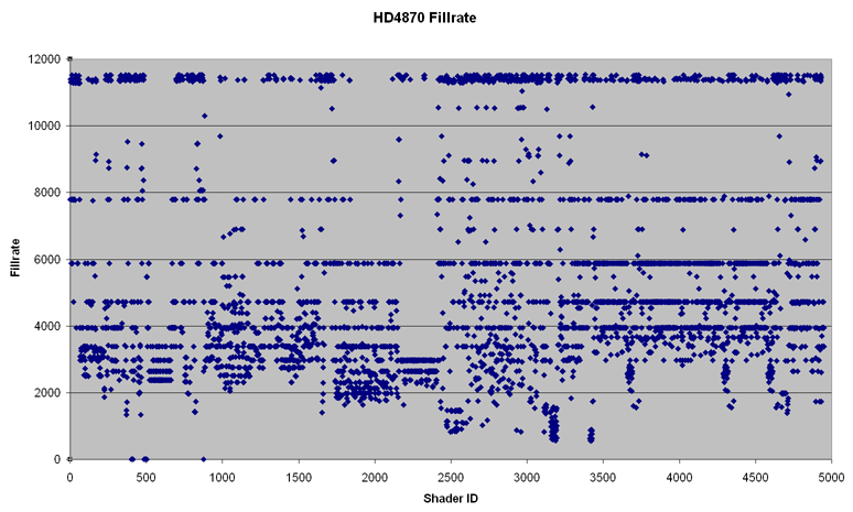
As you can see HD4870's fillrates don't line-up with 750MHz*16=12GP/s:


b3da026.png

Maybe you should check the same driver for all 3 cards? Which sounds like too much hard work to me...

FWIW, here are some GPU-Bench score of HD5870 from my rig (which may be getting already to slow for such a fast card):
I can't find HD4870 numbers :???:

Jawed
 
I can't find HD4870 numbers
RV790 @ 950MHz:
Code:
Instruction Issue
 
512      148.8293       ADD          4         64
512      149.0174       SUB          4         64
512      149.0137       MUL          4         64
512      149.0551       MAD          4         64
512      149.0664       EX2          4         64
512      149.0174       LG2          4         64
512       75.2497       POW          4         64
512      186.2283       FLR          4         64
512      186.0989       FRC          4         64
512      149.0589       RSQ          4         64
512      149.0589       RCP          4         64
512       59.9455       SIN          4         64
512       59.9547       COS          4         64
512      142.4869       SCS          4         64
512      151.3786       DP3          4         64
512      151.4253       DP4          4         64
512      119.5773       XPD          4         64
512      149.0174       CMP          4         64
Code:
Scalar vs Vector Instruction Issue 
 
512      150.9290       ADD          1         40
512      147.3199       ADD          4         40
512      150.9970       SUB          1         40
512      147.2493       SUB          4         40
512      150.9847       MUL          1         40
512      147.3140       MUL          4         40
512      150.9228       MAD          1         40
512      147.3317       MAD          4         40
Windows 7 x86
Catalyst 9.11-beta (v8.670)
 
But they scale very good with core speed over HD4850. Not only good, but almost perfect on average, I'd say.
Thus, one could conclude that bandwidth is not a factor in these performance regions.
As you can see HD4870's fillrates don't line-up with 750MHz*16=12GP/s:


Maybe you should check the same driver for all 3 cards? Which sounds like too much hard work to me...
It's not that hard - actually it's more work to put the spreadsheet together. Speaking of which, in my reviewing, I used the complete set of shaders since this time not only Shaders have doubled but also Raster and ROPs, making much more Shaders "shader limited" I'd guess.

Maybe you can send me your selection criteria (again), so i can try and do both analyses this time 'round.

Btw - the only viable driver would be the HD 5870 Launch driver, which already has been updated (twice if you count in the OpenCL-SDK-Driver from the 8.67 branch), so i'd rather wait at least for the first official Catalyst release.
 
But they scale very good with core speed over HD4850. Not only good, but almost perfect on average, I'd say.
Thus, one could conclude that bandwidth is not a factor in these performance regions.
It's a puzzler. The scaling is key in the analysis I do, so the analysis might need tweaking to take account of something that's "off".

It's not that hard - actually it's more work to put the spreadsheet together. Speaking of which, in my reviewing, I used the complete set of shaders since this time not only Shaders have doubled but also Raster and ROPs, making much more Shaders "shader limited" I'd guess.
The ratios haven't changed with R800, as it's still 10 ALU cycles per pixel of fillrate.

It'll be interesting to see how the deletion of SPI affects things since R800 is interpolating attributes in the shader. Texture coordinates and everything else. That could have some tricky repercussions in the criteria :???:

Maybe you can send me your selection criteria (again), so i can try and do both analyses this time 'round.
The selection criteria depend on what cards you use for your test, e.g. I used HD3870 and 9600GT as a baseline for some criteria.

Btw - the only viable driver would be the HD 5870 Launch driver, which already has been updated (twice if you count in the OpenCL-SDK-Driver from the 8.67 branch), so i'd rather wait at least for the first official Catalyst release.
I think it's best to wait a couple of months for R800 drivers to settle down. At least the GT200 drivers should be decent by now, I imagine the results will be different (3DMark shader tests have varied a lot on GT200). Something like HD4850, HD4870, HD5770, HD5870, GT220, GT240, GTX280 and GTX285 would make for a nice test group.

Then we could repeat a while after Fermi arrives :p

If I re-do the criteria then it would be with the aim of excluding less shaders. Also it'd be nice if some newer games came into the mix.

Jawed
 
I wonder if it's a mistake where it says that Manhattan GPUs for mobile are 32nm? They're listed as 2010 which implies they're Evergreen based (since the GPU before is D3D10.1). The Ontario APU is listed as 40nm, which seems like a mistake too, doesn't it?

Jawed
 
I wonder if it's a mistake where it says that Manhattan GPUs for mobile are 32nm? They're listed as 2010 which implies they're Evergreen based (since the GPU before is D3D10.1). The Ontario APU is listed as 40nm, which seems like a mistake too, doesn't it?

Jawed

And Ati HD5xxx are indicated as ATi 7xx Series.. quite a few mistakes in those slides.
 
I wonder if it's a mistake where it says that Manhattan GPUs for mobile are 32nm? They're listed as 2010 which implies they're Evergreen based (since the GPU before is D3D10.1).
Jawed

I'm pretty sure Evergreen Mobile is 40nm.
 
Back
Top