NocturnDragon
Regular
R700 Fudofacts:
1) 300 Transistors per cell
Those transistors gotta be pretty big!
")
Follow along with the video below to see how to install our site as a web app on your home screen.
Note: This feature may not be available in some browsers.
R700 Fudofacts:
1) 300 Transistors per cell
With PCI Express 2.0 providing 2x the bandwidth per lane, and with the inherently low performance of a $50 part, do you think full 16x lane PCI Express is a priority for a single chip?The low-end part needs full-speed video-decode and should be able to deal with a full-width PCIe connection.
Ah, Fudzilla.
R700 Fudofacts:
1) 300 Transistors per cell
2) Same performance as RV670.
Am I the only one who thinks the two do not add up?
That's probably what you want though, isn't it? Memory system performance should scale with GPU capability. Obviously there are tweaks within performance categories, e.g. between DDR2 and GDDR3 memory speeds.It cannot be disputed that a multi-die solution has a number of inefficiencies that, if at all, can only be overcome by throwing a lot of hardware at it:
- Memory controller area can only scale in lockstep with the amount of shader power
Both of these issues also arise with a monolithic, 400mm2+ GPU. I agree that the "wastage" on multi-chip is higher than with monolithic. It'd be interesting to draw curves for both types and see where they meet - I presume they would meet. 600mm2 for the monolithic GPU? 800mm2?... With leakier, finer, processes presumably the priority is to keep die size down (or "transistor count" down), so perhaps a collection of smaller dies is an advantage?
- inter-die communication will eat up a bunch of die area (and power)
- inter-die access latency will require much larger fifo's across the board
Supposedly ATI already has across-the-die fine-grained redundancy - not just in ALUs/RF but in all the major functional blocks. So ATI doesn't have any more to gain, they've reached the knee on that redundancy graph.Let's take the imaginary number of 4 dies and assume (hope!) that the solution AMD is shooting for is not based on a cooperative software scheme like Crossfire that requires careful per game tuning and inherent inefficiencies.
It's not unreasonable that the total overhead to make all that work efficiently will be 10% compared to single-die solution. 30mm2 is a lot of area to work with to add additional redundancy on a die! Even better: use 5mm2 on the redundancy and the remaining 25mm2 for additional performance.
The same argument applies to the entire history of GPUs as far as I can tell. e.g. I'm convinced that the amount of texturing latency-hiding in the older GPUs - created by having "long pipelines" - was fixed at some "average worst case" and then not scaled as it was implemented across the entire range of GPUs based on that architecture, from the smallest to the biggest, no matter the ratios of ALU:memory clocks, or pipeline-length:typical-texturing latency.Even if AMD goes for the multi-die solution, I can't believe they would use the same chip for the low-end part. There must be tons of elements within a GPU that are sized either for performance or for area efficiency.
It's technically interesting, yeah. But I hate the prospect of the software minefield. I think that's by far the greatest demerit of multi-chip, making all this chip level stuff pale in comparison.With all that, I don't see why I should be excited about multi-die?
Hubba-wa? Can I have some of what you're smoking or can you back up that comparison/statistic in some meaningful way?I think it's similar to the way that GPUs have used "off the shelf" libraries, rather than being "fully custom" - whatever that means. GPUs evolve every 6 months and they have to be implementable at more than one fab with potentially differing libraries. etc. All that stuff has forced GPU design to be "wasteful" in certain parameters - the payoff has been the huge sales (far higher than x86 CPUs in the same time frame).
Hubba-bubba, yep that's gotta be bull, dunno what I was thinking.Hubba-wa? Can I have some of what you're smoking or can you back up that comparison/statistic in some meaningful way?
[/LIST]That's probably what you want though, isn't it? Memory system performance should scale with GPU capability. Obviously there are tweaks within performance categories, e.g. between DDR2 and GDDR3 memory speeds.
Well, no: a monolithic chip will never have inter-die communication overhead.Both of these issues also arise with a monolithic, 400mm2+ GPU.
If the reference point is equal performance, your combination of smaller dies will still be larger, right? So aggregate leakage will be too. What then have your really gained?With leakier, finer, processes presumably the priority is to keep die size down (or "transistor count" down), so perhaps a collection of smaller dies is an advantage?
I think the problem there will be power and heat.What about chip stacking? Does a multi-chip solution have an eye on the future where stacking becomes possible, with the temptation of huge inter-chip bandwidth?
We've discussed the fine-grained redundancy before. Other than for ALU's and memories, I consider it unlikely... (One reason is because I wouldn't know how to do it, which, I admit, is a really weak argument!Supposedly ATI already has across-the-die fine-grained redundancy - not just in ALUs/RF but in all the major functional blocks. So ATI doesn't have any more to gain, they've reached the knee on that redundancy graph.
)The same argument applies to the entire history of GPUs as far as I can tell. e.g. I'm convinced that the amount of texturing latency-hiding in the older GPUs - created by having "long pipelines" - was fixed at some "average worst case" and then not scaled as it was implemented across the entire range of GPUs based on that architecture, from the smallest to the biggest, no matter the ratios of ALU:memory clocks, or pipeline-length:typical-texturing latency.
Ha, yes, I forgot that: it does excite me, but indeed mostly because of technical curiosity.It's technically interesting, yeah. But I hate the prospect of the software minefield. I think that's by far the greatest demerit of multi-chip, making all this chip level stuff pale in comparison.
IBM's new method, which uses current semiconductor manufacturing technology, involves creating tiny holes called "through-silicon-vias" that are etched all the way through a chip and then injected with tungsten to create wires. "This allows us to move 3-D chips from the lab," said Lisa Su, vice president, semiconductor research and development center.
Dave Lammers, director of research for WeSRCH.com, a Web site for semiconductor engineers based in Austin, Texas, said, "Honestly, this is historic. For the first time, we're exploiting the vertical dimension."
Mr. Lammers said there has been considerable discussion about 3-D semiconductors, but no manufacturer had previously said it was ready to start selling chips. He said microprocessor titans Intel Corp. and Advanced Micro Devices Inc. are both believed to be working on 3-D chip technology for future microprocessors, which he predicted will appear in 2009 or 2010.
With PCI Express 2.0 providing 2x the bandwidth per lane, and with the inherently low performance of a $50 part, do you think full 16x lane PCI Express is a priority for a single chip?
I don't.
Jawed
Ok, thx for the response silent_guy. I seem to recall though that AMD was planning a completly new chip design for 2009. I recall whispers of 10 watts a core as the aim - wouldn't that be sufficient to keep heat under control?
http://online.wsj.com/public/article/SB117633745391667111-s93RVktuIlHP3noMcTeax6owiNM_20070419.html
http://www.physorg.com/news95575580.html
G80vG92 is easy to deal with, G92 is bandwidth starved at 2560x1600.I'm not so sure, to be honest. The performance numbers of R600 vs RV670 and G80 vs G92 shows us that memory bandwidth by itself is only part of the equation, right? Dave pointed out that latency related changes were a big factor in the improved performance of RV670.
300M transistors is smaller than RV630 - a part that has "too much" bandwidth (much like R600 though not to quite the same extreme).Let's assume that the single die has a 128-bit memory bus. In this case, your multi-die solution will suffer from the large inter-die latencies, and your single die (which, at 300M transistors, is still a pretty fast part) may be bandwidth starved. Put larger MC's on there and you're 4 die solution will have unused MC's (assuming larger than 512 bits isn't very practical.)
A 128-bit bus is not monolithic - you could deliver SKUs with a 64-bit bus if you want, using only half. One peculiar example of this is RV570/560, two SKUs derived from the same die which is either configured as 256-bit or 128-bit.There's also the thing about redundancy: with a 128-bit bus per die, your granularity options are limited to 1 out of 4 at best, which is quite low. A monolithic chip with a 512-bit bus can have 1 out of 8 granularity or even 1 out of 16 with 32-bit controllers.
Ha, yeah.GDDR5 with 5 GBps per pin may change equations here, of course.
Supposedly one of the benefits of the ring-bus was the removal of hotspots. Seemingly smaller chips are easier to clock higher, which I presume is a hotspot issue. Though I don't have a good understanding of the effects of hotspots on large dies...Well, no: a monolithic chip will never have inter-die communication overhead.
There is really a world of difference between getting a signal across a die and stepping out of bounds. Of the parameters available, you have to assume that at least 1 of them will get worse by an order of magnitude.
If the reference point is equal performance, your combination of smaller dies will still be larger, right? So aggregate leakage will be too. What then have your really gained?
I'm expecting something like micro-channel liquid cooling or something similar to play a part.I think the problem there will be power and heat.
Flip-chip at least provides you with a way to have an equal distribution of power to different parts of the chip. I don't think there's a way to combine die stacking with flip chip (but then I'm not a packaging expert.)
As for heat: you really want some kind of metal in close contact with your die. Here also, die stacking would prevent this.
I can't find the quote where one of the ATI engineers asserts widespread fine-grained redundancyWe've discussed the fine-grained redundancy before. Other than for ALU's and memories, I consider it unlikely... (One reason is because I wouldn't know how to do it, which, I admit, is a really weak argument!
Fine-grained ALU-only redundancy is so 2005...Hence those beasts called HD2600XTx2.The larger the amount of interchangeable identical blocks, the better your ability to tune yield vs performance vs price. There's a world of difference between a 1/4 vs 1/8 granularity. In some perverse way, a larger die can be much more flexible in this way than multiple small ones: if the rumors for 8800GT are true, it was decided late in the game to go from 96 to 112 SP's. You can't decide at the last moment to add another die.
I think the wide-spread fine-grained redundancy makes that moot. Cut-down R600's were/are in very very limited supply. It's either not worth testing/packaging/manufacturing all the combinations (because it was such a runt of a GPU) or the damn thing yielded practically every die as either fully functional or completely bust.R600 has shown little evidence of unit granularity. (If they could, don't you think we'd have seen 448bit version of R600?) So I don't buy there's nothing more to gain.
Yes, RV610 is 2:1 and RV630 is 3:1. RV610 has no L2 cache. RV610 is also incapable of 8xMSAA.Didn't RV610 and RV630 have some differences compared to R600 in terms of shader and texture ratios? RV610 doesn't even have an almighty ring bus! There's differences in video decoders etc. Maybe some caches or other memories are differently sized?
I consider R700 to be a fully distributed GPU. "Master" only relates to a single chip that delivers the completed front buffer for display on your monitor(s). This does mean that the "master" GPU also controls the "gathering" of MSAA data when SuperAA is being performed.I think it is if this low-end chip is also the master for your high-end chip.
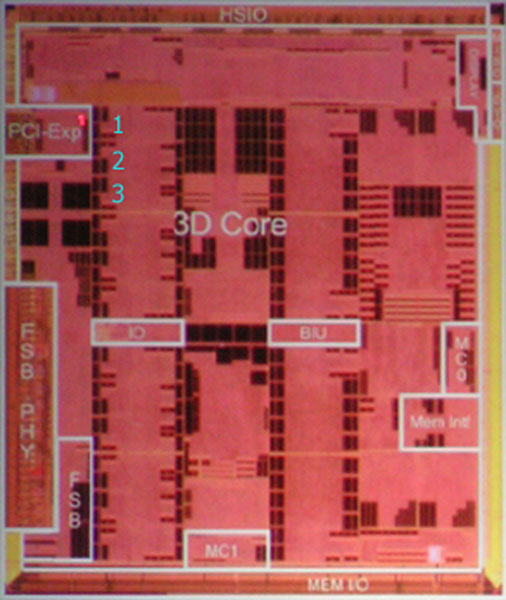
If you look at a die shot of Xenos you'll see that the area labelled "PCI Express" is pretty small - but I don't know how many lanes it is.Does dealing with an x16 link split across multiple chips, or splitting a command stream across multiple x8/x4 links really make much sense? And how much does a full x16 link cost in the scheme of things?