AMD: R7xx Speculation

Status
Not open for further replies.
whats the general consensus of die size % of the ALU in the rv670?

If they were to put in 800 SP's, thats what 160 vec 5 shaders? A 2.5 times increase, with only a 25% increase in the current die size, thats just not possible if the SP's in the rv670 takes over 50% unless die size is off too, which at this point I really don't think its off unless the pro and xt are different chips. And this is without any other changes in the rv670. And the TDP figures would be off too if this was the case..... I mean we would have to throw everything out :runaway:
 
Is the bridge chip being used just a standard 3rd party PCI-E controller or something AMD is making on their own?

From some of the past chipsets that were released, ATI was incorporating fast data paths between two devices connected to the controller. Could they be using something similar built onto the card to act as the bridge. That would definitely cut back on latency and increase bandwidth between the two cards since the data would no longer be constrained by the PCI-E bus. They could incorporate well over 16 lanes between the cards if they needed the bandwidth.

Also why add another stop on the bus to get to the outside world when they could just beef up the one already on the chip? The downside that comes to mind is one additional hop for getting data to and from the card itself. Communication between the two cores on the other hand would be significantly improved if that was a bottleneck before.

Also with a bridge chip included they could also incorporate any external interface they desired into the chips. So HTX or some other communication method between chips and PCI-E to connect to the system.

Well my thoughts about AMD/ATi using PEX8547 was that they weren't looking into a long term investment by going with the Gen1 chip rather than the PEX8648. That lead me to assume they were either working on their own or heard/working on something better.
 
whats the general consensus of die size % of the ALU in the rv670?

If they were to put in 800 SP's, thats what 160 vec 5 shaders? A 2.5 times increase, with only a 25% increase in the current die size, thats just not possible if the SP's in the rv670 takes over 50% unless die size is off too, which at this point I really don't think its off unless the pro and xt are different chips. And this is without any other changes in the rv670. And the TDP figures would be off too if this was the case..... I mean we would have to throw everything out :runaway:

maybe 480+320=800
 
whats the general consensus of die size % of the ALU in the rv670?

If they were to put in 800 SP's, thats what 160 vec 5 shaders? A 2.5 times increase, with only a 25% increase in the current die size, thats just not possible if the SP's in the rv670 takes over 50% unless die size is off too, which at this point I really don't think its off unless the pro and xt are different chips. And this is without any other changes in the rv670. And the TDP figures would be off too if this was the case..... I mean we would have to throw everything out :runaway:
K, I'm thick, lets try the high school math:
(1)1.25*(a+s) = (a+2.5s)
(2) a+s = 1
(2a) a=1-s
(2a in 1) 1.25 = 1-s+2.5s
1.25 = 1+1.5s
0.25 = 1.5s
(1/4)*(2/3) = s
s = 1/6 = 0.1666 = 16.6%

<salt>So the original shaders take 16.6% of rv670's size.</salt>
It's 55nm, with 1Mbyte cache. Dont know if that register file is comparable to normal CPU SRAM cache. Anyone with die porn shots? We could compare to say C2D pr0n on 65nm to guesstimate. Whats a c2d in mm2? Whats the rv670 im mm2?
 
[...]So yeah, call me crazy, but I'm still giving a 65%+ chance of RV770 being monolithic (350mm²+) *shrugs*. Might be usable for a X2 with some units disabled down the line though, who knows.

Once again, I could be horribly wrong here, but I wouldn't have been surprised at all if the everyone has been misled. This would hardly be unprecedented in the history of the industry either so I don't think it'd be horribly surprising...
Do you think, that Mr. Pande from Stanford's F@H has also been mislead, optimizing newer folding cores for 480 SPs instead of 800 gazillion Vec16 units?


I believe that simple cherry-picking of 4xMSAA benchmarks with RV770 specified as 480 ALU lanes, 16 TUs, 16 RBEs (with 4x Z per clock) is all that AMD needs to claim the performance gains they're indicating.
I concur - unfortunately.
 
As to Kyle's comment in AnarchX's Link: How can AMD possibly "fix" FSAA it's not broken at all?
 
As to Kyle's comment in AnarchX's Link: How can AMD possibly "fix" FSAA it's not broken at all?


I agree, but what about the part of performance with AA on in DX10? Problem or not, that has to get remedied fast.

Unless DX10 games have had a greater Z-fillrate demand of magnitudes more just with AA on, I'm not seeing the whole reason fit.
 
I agree, but what about the part of performance with AA on in DX10? Problem or not, that has to get remedied fast.

Unless DX10 games have had a greater Z-fillrate demand of magnitudes more just with AA on, I'm not seeing the whole reason fit.

What performance with AA on DX10?The performance drop associated with enabling AA is similar across APIs (in the same games, of course).
 
The chip still has to be setup and receive commands from the host, simply reading and writing on the ring bus won't let you do that.
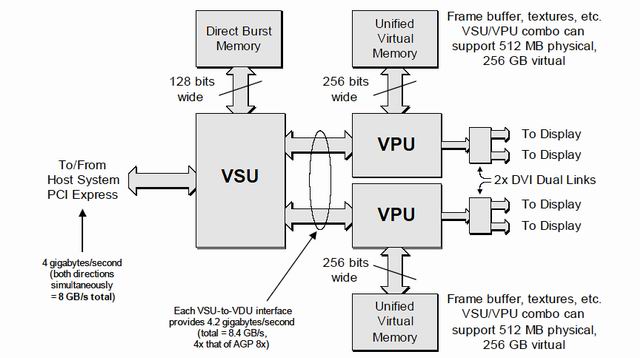
I was hoping there'd be a branch dedicated to inter-chip comms, separate from the branch dedicated to PCI Express:

Code:
    MC        MC    MC        MC
      \------/        \------/
      |      |  bri   |      |
-------      ==========      -------
|     |      |  dge   |      |     |
|     /------\        /------\     |
|   MC        MC    MC        MC   |
|                                  |
|                                  |
----------------    ----------------
PCI Express    |    |    PCI Express
                CPU


You could just replicate the textures (except for the rendered ones).
Since textures normally consume hundreds of MB doing that would nullify most of the benefit of sharing.

Jawed
 
like this
l_kn_vsu_vpu2.jpg
 
<salt>So the original shaders take 16.6% of rv670's size.</salt>
It's 55nm, with 1Mbyte cache. Dont know if that register file is comparable to normal CPU SRAM cache. Anyone with die porn shots? We could compare to say C2D pr0n on 65nm to guesstimate. Whats a c2d in mm2? Whats the rv670 im mm2?
RV670 is 192mm2 with 666M transistors. 16.6% of 666M is 111M transistors. The 1MB register file is 3-ported (according to the R600 ISA), implying that it's really 3MB.

Anyway, for 111M transistors, that would imply that each "pixel" (there being 64) costs about 1.75M transistors, cheaper than R5xx's 1.9M transistors - which, to be honest, seems unlikely. I guess 3M for what it's worth.

This is the closest you'll get to a die shot that shows anything:

http://www.anandtech.com/video/showdoc.aspx?i=3151

The RV670 die looks suspiciously like R600 shrunk, not taking account of the different MC configuration - in other words, misleading. Of course it could be the "R600" shot is really RV670 scaled up. Sigh.

Jawed
 
All the indications are that RV770 will be significantly less than 2x the performance of RV670.
Jawed


If it's 1.25 9800GTX which is the common rumor, it's already ~2x RV670.

People probably dont realize how much faster 9800GTX is than 3870. In Crysis for example it's approaching double.
 
Last edited by a moderator:
Jawed said:
All the indications are that RV770 will be significantly less than 2x the performance of RV670.
If it's 1.25 9800GTX which is the common rumor, it's already ~2x RV670.
I have gut feeling Jawed is right for most situations. But of course there probably are benches where RV770 reaches 2x. 3DMark06 for example ;).
 
Status
Not open for further replies.
Back
Top