AMD: Pirate Islands (R* 3** series) Speculation/Rumor Thread

290X GPU cards are cooled just fine with air, so no problem on that front. Water just complicates things, like how do you run such a setup in crossfire? It'll be difficult to find room to fit the second radiator.
I agree with issues regarding crossfire/sli & multiple radiators .... hopefully we will see some external solutions similar to what Gigabyte introduced, and if possible a barebones implementation (supply your own GPU's).
http://www.guru3d.com/articles-pages/geforce-gtx-980-waterforce-3-way-sli-review,4.html
 
Looks a bit too good to be true but maybe AMD has a real winner card there.
Looks exactly what we could expect for a 28nm part IMO. They're dealing with the same size constraints as Nvidia, so roughly 600mm2. That caps the performance increase to about 50% for the same architecture, but with an unknown upside bonus for removing BW bottlenecks. Perf/W improvements due to HBM as well, but again nothing spectacular.
This thing won't blow gm200 out of the water at all, but will be quite a bit more expensive to make.
Should be a very competitive GPU for games and an amazing one for BW limited compute, but I don't see the real winner part yet.
 
...it is a necessity - to not have bad reviews just for the noise (one would think it doesnt matter in reference design but it is, according to reviewers..) and -maybe- put slightly higher default clock?

If they use this time a better fan on the radiator....

I agree with issues regarding crossfire/sli & multiple radiators .... hopefully we will see some external solutions similar to what Gigabyte introduced, and if possible a barebones implementation (supply your own GPU's).
http://www.guru3d.com/articles-pages/geforce-gtx-980-waterforce-3-way-sli-review,4.html

With todays CPU ( 6-8cores ) and high end gpu's, better to go for a good custom watercooling setup for dual/ triple gpu's.
 
I'm speculating without a solid basis, but if HBM is in the design, perhaps the water cooler is there because the DRAM is up close and personal with a ~200-250W slab of silicon? HBM does discuss pretty high thermal thresholds, measures like temperature-compensating refresh rates, and structural measures like dummy bumps and pillars to allow thermal dissipation in the stack, but it may not like the high temperature target that AMD has sort of designed itself into with its otherwise rather effective GPU power monitoring.

The following (not quite the same thing, but related given the authorship) seems to put a desired ceiling of 85 C for DRAM, and there's the matter of a significantly more dense thermal footprint with the chip package hosting so much silicon.
http://www.cs.utah.edu/wondp/eckert.pdf

Was there a clear shot of an external radiator for the rumored cooler?
 
Was there a clear shot of an external radiator for the rumored cooler?

The only one i remember, had only the metal case.

AMD-Radeon-R9-390X-cooling.jpg
 
Are the slots in the rumored single-GPU cooler sufficiently wide for tubing? There seems to be metal running through the gap in the silver exterior where the 295x2's shroud had enough room for tubing and wiring.

Cooler aside, if HBM were in a top product, if there isn't a higher-capacity storage pool, the known HBM densities would be problematic unless something like the 20nm-class doubling of GDDR5's density could carry over to a surprise revision of HBM Gen1.
 
Cooler aside, if HBM were in a top product, if there isn't a higher-capacity storage pool, the known HBM densities would be problematic unless something like the 20nm-class doubling of GDDR5's density could carry over to a surprise revision of HBM Gen1.

Yeah... Kinda makes me think it'll be introduced in a lower-end SKU, but that makes it weird with costs (can't be that cheap?).

Any idea how much pad space these stacks would even take to hook up to a chip? I'm not clear on what's feasible, like, if 4 separate stacks would require a really fat chip or.... :?:
 
The test modules had one big chip with two sides bounded by two smaller die each. The old photos had it arranged in an L shape, which would probably favor a more square die, with its dimensions apparently correlating to the the length of the area set aside for the memory modules.

There are abstract diagrams of a large die flanked on two opposite sides by memory, which would theoretically allow for the GPU to be more flexible along one axis. The interposer itself imposes limits, so even if pad space is not the limiter, the interposer now makes the area of the GPU+memory more valuable than it used to be.
 
Erm.. if HBM is used, isn't the PCB going to be significantly smaller on all the cards using that tech?
I imagined the R380's PCB being small enough to fit into a mini-ITX case.

Am I wrong?
 
This thing won't blow gm200 out of the water at all, but will be quite a bit more expensive to make.
Should be a very competitive GPU for games and an amazing one for BW limited compute, but I don't see the real winner part yet.
Presumably AMD is going to continue putting full-speed DP into its enthusiast chips, whereas it seems NVidia won't. So I think we can assume AMD's decided never to be king of the hill once both enthusiast chips from the same "generation" are on the market (once we could use fab node to define generation, but the wheels have fallen off).

I can't see how this rumoured card is 50% faster than 290X if it has ~double the bandwidth + Tonga style improved bandwidth efficiency. It's simply too slow.

I would expect 290X with Tonga-efficiency improvements and no other changes to perform ~50% better at the same power (OK, it might need more ROPs...).

I really can't see how this is an HBM card. The performance margin is tragic.

EDIT: What's the lowest bandwidth we can expect for 4GB of HBM?
 
Last edited:
Presumably AMD is going to continue putting full-speed DP into its enthusiast chips, whereas it seems NVidia won't. So I think we can assume AMD's decided never to be king of the hill once both enthusiast chips from the same "generation" are on the market (once we could use fab node to define generation, but the wheels have fallen off).

I can't see how this rumoured card is 50% faster than 290X if it has ~double the bandwidth + Tonga style improved bandwidth efficiency. It's simply too slow.

I would expect 290X with Tonga-efficiency improvements and no other changes to perform ~50% better at the same power (OK, it might need more ROPs...).

I really can't see how this is an HBM card. The performance margin is tragic.

EDIT: What's the lowest bandwidth we can expect for 4GB of HBM?

I think 4GB would mean four 1024-bit stacks of 1GB, probably running somewhere between 800MHz and 1200MHz, based on what little information is currently available. So 409.6GB/s to 614.4GB/s. But I don't think HBM alone would bring all that much of a performance boost, since Hawaii never looked all that bandwidth-limited to me. As for Tonga's improvements, they've never been properly quantified (as far as I know).
 
I'm speculating without a solid basis, but if HBM is in the design, perhaps the water cooler is there because the DRAM is up close and personal with a ~200-250W slab of silicon? HBM does discuss pretty high thermal thresholds, measures like temperature-compensating refresh rates, and structural measures like dummy bumps and pillars to allow thermal dissipation in the stack, but it may not like the high temperature target that AMD has sort of designed itself into with its otherwise rather effective GPU power monitoring.

The following (not quite the same thing, but related given the authorship) seems to put a desired ceiling of 85 C for DRAM, and there's the matter of a significantly more dense thermal footprint with the chip package hosting so much silicon.
http://www.cs.utah.edu/wondp/eckert.pdf

Was there a clear shot of an external radiator for the rumored cooler?
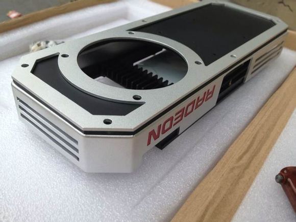
Wouldn't it be easier to thermally decouple the GPU and the DRAM chips using the cooler?

I mean, you could have a block of copper/nickel on top of the GPU, with heatpipes connected to aluminum fins, and separate blocks of copper/nickel on top of the DRAM stacks, with their own heatpipes leading to a different set of aluminum fins. The fan(s) could still blow on all fins at once.

Wouldn't that keep the RAM acceptably cool without having to worry too much about the heat generated by the GPU?

For some of the prototype photos, the DRAM chips look to be few millimeters at most from the side of the GPU, which in a standard setup provides a decent amount of uniform metal for the cooler's base.
(edit: cut off the end of the previous sentence somehow )
The mechanical aspect of the cooler and its baseplate/mountings would be interesting to see. In terms of manufacturing, it sounds notably more complex to build.
If it's not isolated enough, the DRAM chips would look like a tempting sink for the GPU's output with 15 C or more difference in temperature.

Thermally, I'm curious if there could be concerns if part of the interposer is significantly cooler than something immediately adjacent. If the cooler keeps things closer to equivalent over the whole package, there would be less concern for long-term reliability.
 
Last edited:
Erm.. if HBM is used, isn't the PCB going to be significantly smaller on all the cards using that tech?
I imagined the R380's PCB being small enough to fit into a mini-ITX case.

Am I wrong?
I believe, ideally, it should be smaller. In reality, with the supposed high power consumption of Fiji, you have to take into consideration the size of the cooler.
Obviously, hybrid water/air means you don't need a large heatsink meant for the full TDP.

The one exception that pops out is the GTX670, there were some interesting aftermarket options that shrunk everything way down, but even the reference with the "small" PCB still had to take up more room since the fan/heatsink went over the edge of the PCB.


The small PCB in the GTX670 was actually nVidia's own standard design. The long models actually came afterwards when the 3rd parties tried to cram better/bigger voltage regulators.
I was actually only talking about the Fiji's PCB. Either the cooler makes it into a longer card is another thing, but at least the PCB should be a lot smaller.
 
I can't see how this rumoured card is 50% faster than 290X if it has ~double the bandwidth + Tonga style improved bandwidth efficiency. It's simply too slow.
Going by the current rumors, Fiji will have 4096 ALUs which is 45% more than Hawaii. The Firestrike performance increase is +63%. The game performance is +51%. It depends on how BW limited R9 290X really was, but it seems too slow.

EDIT: What's the lowest bandwidth we can expect for 4GB of HBM?
First gen HBM should be 128GB/s per stack, according to these Hynix slides.
 
Back
Top