3D Technology & Architecture

Ok, so basically, that's all related GS and/or streamout? Yes, that makes perfect sense.

I think that's a big portion of it.

Future API plans seem to include more feedback in the system, and GPGPU would include algorithms that might want more passes over data or other more general kinds of memory usage.
 
Maybe there are other candidates that profit more from a cache, where latency hiding is harder? If there were no L2 caches in previous generations (?), are there features in DX10 that make a cache more useful?
Older GPUs have other kinds of caches, not just texture caches. e.g. ATI GPUs have a colour buffer cache (render target) and a z/stencil buffer cache.

There's also the post-transform vertex cache that is titchy (10s of vertices in size, a few hundred bytes, perhaps as much as 1KB, effectively).

R600 seems to be ATI's first GPU with an L2 cache, for what it's worth. NVidia has had L2 since at least NV40. Earlier than that is too far back in time for me.

The use of the screen-space tiled rasterisation of triangles in R300 and later meant that there was little need for L2. Obviously texels overlap a bit at tile boundaries, but if the tiles are reasonably big, e.g. 256 pixels, then I suppose the high-cost texels tend to be constrained within single tiles.

At least in ATI's old texturing system, anyway. Clearly the R600 texturing system is vastly more complex.

Really you could say that D3D10 introduces more sources of latency into the GPU pipeline. A nice example is constants, where you can have multiple fairly complex struct arrays defined, each arbitrarily addressed at random times during shading.

And then there's the explicit looping that 3dilletante refers to.

Jawed
 
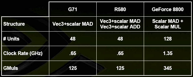
Who doesn't? 128 stream processors at 1.35 GHz is 346 GFLOPS...

There was some confusion a while back about how Nvidia was marketing G80. In the review guide they referred to a 518Gflop count (including the missing MUL). So it wasn't clear if their recent claim of 1TFLOP was using this same logic (including the missing MUL). If they are consistently ignoring the MUL that paints G92 in a much better light.
 
The muxes/demuxes/buses needed to move data around in a chip is the most overlooked aspect of chip design on these forums. The actual arithmetic logic (esp. single precision) isn't very costly to implement.

The register file needs very high bandwidth (80 sp * 3+1 I/O * 32 bits = 10 kbits per clock, and this for each quarter of R600!) and very fine granularity in the data it moves.


As for the talk about caches, the reason GPUs have so many pixels in flight is that they don't need to rely on caches. They load the data as it's needed and are willing to wait for it. The cache is just there to minimize redundant loading which costs bandwidth. R600 has plenty of pixels in flight as well as bandwidth, so I'm not sure why they put so much cache on there. Maybe hundreds of kilobytes on a 700M transistor chip is so relatively small that the tiny benefits are worth it.

To minimize bandwidth usage with 16xAF, though, you need at least 16 * (no. of pixels in flight) * (textures in the shader) texels in the cache. That's quite a bit, but for that kind of workload you don't really care if have a little redundant texture loading, especially with 141 bytes per clock to share among only 16 TMUs.
 
There's also the post-transform vertex cache that is titchy (10s of vertices in size, a few hundred bytes, perhaps as much as 1KB, effectively).
Tipically these caches contain ~20 vertices, now IIRC SM4.0 let you output 16 vec4 so that you need ~300 bytes to store a single vertex worth of post transformed data (if we include position and color(s) as well..).
I'm quite sure that post transformed caches are way bigger than 1 kb in SM3.0 and SM4.0 GPUs
 
There are probably other issues with drivers and hardware bugs, though the glaring fill rate and filtering shortfalls look to be responsible for a lot.

That being said, ATI has been pretty consistent about the idea that they push "quality pixels" as opposed to raw output numbers.

R600 isn't the first ATI chip to run into problems where some popular games failed to meet the design's expectation for heavier ALU usage.
 
Tipically these caches contain ~20 vertices, now IIRC SM4.0 let you output 16 vec4 so that you need ~300 bytes to store a single vertex worth of post transformed data (if we include position and color(s) as well..).
I'm quite sure that post transformed caches are way bigger than 1 kb in SM3.0 and SM4.0 GPUs
Aha, I thought under SM3 a typical vertex was around 20 bytes and there were about 20 of them... Hmm, seems I was thinking of the input data per vertex, not the output data, including attributes. Sigh.

R600 appears to use the memory read/write cache as an "overspill" for PVTC. I'm fairly skeptical about this lickle 8KB cache (per SIMD) because it's doing a whole load of other stuff too.

Jawed
 
Is it that simple? But then why would the ATI engineering team over look texture rate and fillrate? Did they just misjudge what games would be using in the future?
TUs and RBEs take a lot of transistors. Put bluntly, to scale their quantity costs prolly hundreds of millions of transistors when you're dealing with a GPU of the scale of R600. That's because you can't just add another 6 TUs, or another 2 RBEs. The 4-way "symmetry" of R600 means that TUs and RBEs need to come in 16s. Ouch.

Also, I think ATI spent a monster amount of die space on virtual memory, ring bus/512-bit memory bus, caching, multiple concurrent contexts, localised thread control processors and the register file. These are infrastructural concepts that have a high cost of entry (like dynamic branching in R5xx has a high cost - a cost that also paid-back in terms of texturing performance though). When you've done all that good stuff, there isn't the room to put in a monster amount of TUs and RBEs.

I see a lot of architectural infrastructure that's "ready" for D3D10.1/11. Maybe those are rose-tinted glasses.

Arguably ATI is paying too much upfront. But until the drivers are sane, how are we supposed to tell. How long before we get bored waiting for sensible high-IQ performance?

Jawed
 
I don't see how die-space hungry oversized memory controller and ring bus are "forward-looking infrastructural costs" that will make R6xx more "D3D10.1/11-ready" than the competing design.
 
I don't see how die-space hungry oversized memory controller and ring bus are "forward-looking infrastructural costs" that will make R6xx more "D3D10.1/11-ready" than the competing design.
Those things appear to be intrinsic to ATI's conception of a GPU. I say that on the basis of a multitude of patent documents, and the virtual memory gubbins is, I think, the foundation of the architecture.

I think D3D11 is the point at which the CPU gains complete control over the GPU's use of memory, and I believe that ATI has architected R600 on that basis. It'd be nice if there were some white papers on this subject, or an interview that went into the nitty gritty, but well I'm left with these interpretations...

Jawed
 
There was some confusion a while back about how Nvidia was marketing G80. In the review guide they referred to a 518Gflop count (including the missing MUL). So it wasn't clear if their recent claim of 1TFLOP was using this same logic (including the missing MUL). If they are consistently ignoring the MUL that paints G92 in a much better light.
I never saw any NVIDIA marketing talking about 518 GFLOPS.

Anyway, the current consensus is that the SFUs can perform a MUL in 4 clock cycles per quad. This puts a GTX at 398 GFLOPS. So even if the 1 TFLOPS for G92 is with the MUL included (assuming the exact same stream processor architecture as G80), it doesn't matter much.
 
Tipically these caches contain ~20 vertices, now IIRC SM4.0 let you output 16 vec4 so that you need ~300 bytes to store a single vertex worth of post transformed data (if we include position and color(s) as well..).
I'm quite sure that post transformed caches are way bigger than 1 kb in SM3.0 and SM4.0 GPUs
SM4.0 actually lets you output 32 vec4's per vertex from the GS, 16 from the VS.
 
I never saw any NVIDIA marketing talking about 518 GFLOPS.
Irrespective of what its actually doing, every review characterises each ALU as MADD+MUL co-issue cabaple, which puts it at 518GFLOPs.

g80-dia-4.png

Thats indicating that two MUL's could be issued per cycle per shader.
 
Irrespective of what its actually doing, every review characterises each ALU as MADD+MUL co-issue cabaple, which puts it at 518GFLOPs.

g80-dia-4.png

Thats indicating that two MUL's could be issued per cycle per shader.
And that is positively not the case?
 
Back
Top