Are people normalising prices for inflation?
You are using an out of date browser. It may not display this or other websites correctly.
You should upgrade or use an alternative browser.
You should upgrade or use an alternative browser.
Cost of advanced chip manufacture
- Thread starter IQandHDR
- Start date
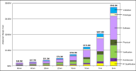
These wafer calculators are very basic. and never represent the reality. For example, I can say, that in midlife term, so 1 year after launch, AD102 yields were above 90%. Because there are many methods of getting yields above what the calculator says like dark silicon, redundant blocks, and salvaged dies for lower SKUs48 good dies per wafer from the link I posted but that does not take into account redundancy, salvageability, parametric yields as mentioned by @arandomguy. If I take another calculator I get 50 dies so it's in the same range - http://cloud.mooreelite.com/tools/die-yield-calculator/index.html
View attachment 12424
However, this is very simplistic and there are many more optimizations you can make including die shape, redundancy, product planning/salvageability to maximize use of chips.
AD102-300 (RTX 4090) is 87.5% of a full AD120 die. (0.91% on Steam)
AD102-175-KEF-A1 (RTX 4070 Ti Super) is 45.8% (0.52% on Steam)
If that +90% yield include dies that are only 45,8% of a full die that numbers is really not very telling.
But then again, I guess is better to recoup some cost on the AD102-175-KEF-A1 dies, than a "blanket loss".
AD102-175-KEF-A1 (RTX 4070 Ti Super) is 45.8% (0.52% on Steam)
If that +90% yield include dies that are only 45,8% of a full die that numbers is really not very telling.
But then again, I guess is better to recoup some cost on the AD102-175-KEF-A1 dies, than a "blanket loss".
Only a tiny fraction of 4070 Ti supers are AD102. Most are AD103 (specifically AD103-275-A1)AD102-300 (RTX 4090) is 87.5% of a full AD120 die. (0.91% on Steam)
AD102-175-KEF-A1 (RTX 4070 Ti Super) is 45.8% (0.52% on Steam)
If that +90% yield include dies that are only 45,8% of a full die that numbers is really not very telling.
But then again, I guess is better to recoup some cost on the AD102-175-KEF-A1 dies, than a "blanket loss".
AD102-300 (RTX 4090) is 87.5% of a full AD120 die. (0.91% on Steam)
AD102-175-KEF-A1 (RTX 4070 Ti Super) is 45.8% (0.52% on Steam)
The 4070 Ti Super was released long after the 4090. Steam comparisons don’t make sense. Besides the 4070 Ti super is based on AD103.
Most models are indeed AD103, I think 2 other models are AD102 from I can gather.The 4070 Ti Super was released long after the 4090. Steam comparisons don’t make sense. Besides the 4070 Ti super is based on AD103.
my data was before 4070Ti launch. I didn't get an update but an educational guess would put this number above 99% if taking into account salvaged dies used on 4070TiAD102-300 (RTX 4090) is 87.5% of a full AD120 die. (0.91% on Steam)
AD102-175-KEF-A1 (RTX 4070 Ti Super) is 45.8% (0.52% on Steam)
If that +90% yield include dies that are only 45,8% of a full die that numbers is really not very telling.
But then again, I guess is better to recoup some cost on the AD102-175-KEF-A1 dies, than a "blanket loss".
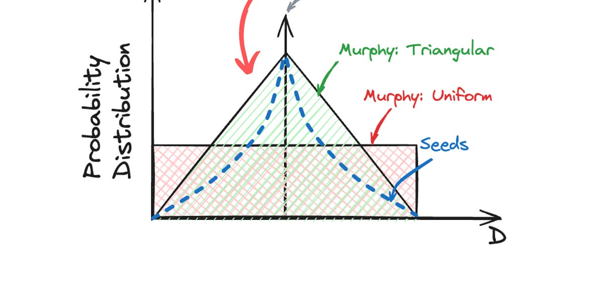
+99% die rate sounds rather high when looking at this:
 www.viksnewsletter.com
They stop at ~90% success rate, what do you base your numbers on?

How Foundries Calculate Die Yield
Understanding the metric that Intel used to abandon a whole technology node.
They stop at ~90% success rate, what do you base your numbers on?
First D0 is below 0.07 at TSMC mature 5nm class process+99% die rate sounds rather high when looking at this:

How Foundries Calculate Die Yield
Understanding the metric that Intel used to abandon a whole technology node.www.viksnewsletter.com
They stop at ~90% success rate, what do you base your numbers on?
And most important, a defective die can still be used, thanks to redundant areas, dark silicon and entire blocks (where sits the defect) that can be de-activated when making salvaged SKU.
In fact 99% is nothing special. I've seen 99.7% on a 7nm ARM industrial APU project that included a bit of redundancy.
In regards to yields:

 wccftech.com

"Ousted" Intel CEO Steps In To Defend The Firm's 18A Process, Says Yield Rate % Isn't The Right Metric To Measure Semiconductor Progress
Intel's former CEO Pat Gelsinger arrived on the scene, defending 18A "yield rate" claims by saying that the team is "doing incredible work".
I had posted about it in the Intel thread as well
Why does anybody pay attention when any of these "news" outlets mention "yields". What yields? For which parts?
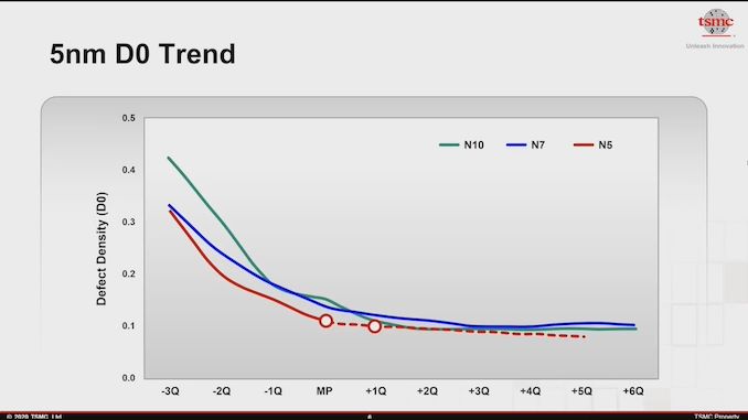
Intel has publicly mentioned that the D0 for 18A is under 0.4, and at that point it was like a year to mass production. For comparison for TSMC, D0 for N5 and N7 was ~0.3-0.35 at 3Q before mass production.
3nm was known when TSMC published the technical details, and TSMC somewhat pushed finfets as much as they could, with the SRAM not scaling being a drawback. But they went for maturity over rushing new transistor tech before they thought it was fully ready for mass production (we can see how that worked out for Samsung). But it was never expected not to scale any further, just that going forward it would scale much less vs logic.
Either ways though, whether it scales or not, the higher cost of the new nodes will itself make using more SRAM challenging for all but the highest margin chips. So having tech like AMD's will be an advantage.
Cross posting from the AMD thread since the discussion is more relevant here @Kaotik
As per presentations at IDEM, CFET's are expected to be introduced from the "A7" node onwards, which should follow "A14" (A16?) and "A10", if we take a 2 year cadence, A10 should be in the H2 2028 timeframe and then A7 in the H2 2030 timeframe at the earliest -

The interesting bit is that CFET's could bring a 1.5-2X scaling in SRAM density -

D
Deleted member 87499
Guest
Cross posting from the AMD thread since the discussion is more relevant here @Kaotik
As per presentations at IDEM, CFET's are expected to be introduced from the "A7" node onwards, which should follow "A14" (A16?) and "A10", if we take a 2 year cadence, A10 should be in the H2 2028 timeframe and then A7 in the H2 2030 timeframe at the earliest -

The interesting bit is that CFET's could bring a 1.5-2X scaling in SRAM density -

This post is gold.
Similar threads
- Replies
- 34
- Views
- 5K
- Replies
- 21
- Views
- 3K
- Replies
- 75
- Views
- 14K
D
- Replies
- 70
- Views
- 21K
- Replies
- 188
- Views
- 33K

