Sony PlayStation 5 Pro

In that case, it would've been lovely to get some Infinity Cache in the Pro for exactly this reason. Especially for 700 bloody quid.
More cache ala Infinity Cache isn't necessarily better here. If you look at this Cheese and Chips article L1 hit rate is really low as is the Infinity Cache (top bar).

The cache setups are likely different with RDNA 4 given the deep dive of results below. L1 just isn't performing, (it's also read only). L2 needs to be much larger as a working cache, but it's further away, and the L3 (infinity cache) doesn't seem to add that much benefit.

There's not really a good solution here for consoles, the price/cost point of consoles restricts how much can be spent. At the end of the day, the caches that are available for use, to optimize performance from these consoles, developers will need to figure out a way to get better hit rates on their caches, and the platforms have to provide the tools to enable them to do that.
Screenshot 2024-09-26 at 7.30.04 AM.png
 
So Cerny's "custom hardware for machine learning" is just some tweak to the CUs? I'd consider that false advertising.
From Cheese and Chips overlooking RDNA 4 in the llvm. This article was dated back in January 2024.


Sparsity​

Moving to lower precision data formats is one way to scale matrix multiplication performance beyond what process node and memory bandwidth improvements alone would allow. Specialized handling for sparse matrices is another way to dramatically improve performance. Matrices with a lot of zero elements are known as sparse matrices. Multiplying sparse matrices can involve a lot less math because any multiplication involving zero can be skipped. Storage and bandwidth consumption can be reduced too because the matrix can be stored in a compressed format.

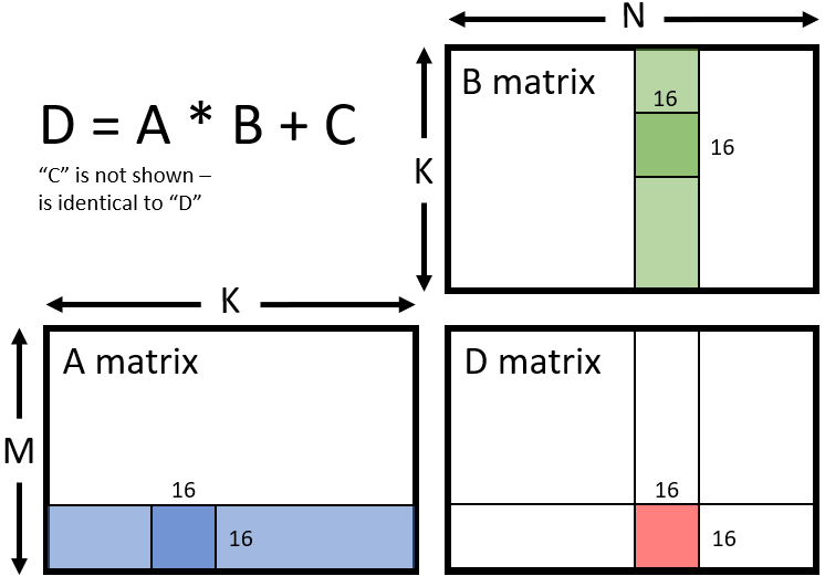
RDNA 4 introduces new SWMMAC (Sparse Wave Matrix Multiply Accumulate) instructions to take advantage of sparsity. SWMMAC similarly does a C += A * B operation, but A is a sparse matrix stored in half of B’s size. A sparsity index is passed as a fourth parameter to help interpret A as a full size matrix. My interpretation of this is that the dimensions in the instruction mnemonic refer to stored matrix sizes. Thus a 16x16x32 SWMMAC instruction actually multiplies a 32×16 sparse matrix with a 16×32 dense one, producing a 32×32 result.

InstructionMultiplied Matrices (A and B) FormatResult/Accumulate Format
V_SWMMAC_F32_16X16X32_F16FP16
A: 16×16 stored/32×16 actual
B: 16×32
32×32 FP32
V_SWMMAC_F32_16X16X32_BF16BF16FP32
V_SWMMAC_F16_16X16X32_F16FP16FP16
V_SWMMAC_BF16_16X16X32_BF16BF16BF16
V_SWMMAC_I32_16X16X32_IU8INT8INT32
V_SWMMAC_I32_16X16X32_IU4INT4INT32
V_SWMMAC_I32_16X16X64_IU4INT4
A: 16×16 stored/32×16 actual
B: 16×64
32×64 INT32
V_SWMMAC_F32_16X16X32_FP8_FP8FP8FP32
V_SWMMAC_F32_16X16X32_FP8_BF8FP8 and BF8FP32
V_SWMMAC_F32_16X16X32_BF8_FP8BF8 and FP8FP32
V_SWMMAC_F32_16X16X32_BF8_BF8BF8FP32
If I guessed right, SWMMAC instructions would be the same as their WMMA siblings, but produce a result matrix twice as long in each dimension.

Of course there’s no way to infer performance changes from looking at LLVM code, but I wonder if AMD will invest in higher per-SIMD matrix multiplication performance in RDNA 4. RDNA 3’s WMMA instructions provide the same theoretical throughput as using dot product instructions.

[WMMA] instructions work over multiple cycles to compute the result matrix and internally use the DOT instructions
“RDNA 3” Instruction Set Architecture Reference Guide
Since SWMMAC takes a sparse matrix where only half the elements are stored, perhaps RDNA 4 can get a 2x performance increase from sparsity.
 
DLSS/XESS and PSSR(probaly) uses int8
Why int8 is most likely:
1)Xess providing comparable quality to dlss on intel ARC uses int8
https://www.tomshardware.com/news/intel-xess-technology-demo-and-overview

2)Int8 is accelerated by all nvidia GPUs from turing and above

3)Alex Battaglia said DLSS uses int8

The Int8 rate of RDNA2/3 is the same and it is very low compared to turing
2070=126tops
7900xt=103tops
Dlss-like NN is not possible on RDNA3 GPU with acceptable speed
Either Sony has made some other changes to the architecture besides the new RT blocks
Either some kind of coprocessor or a separate asic is used in the gpu
Thanks for the input, I hadn't seen that article and there isnt much information about DLSS in the wild. If it is int8, then arent the more relevant numbers the dp4a versions, not wmma? So the RDNA3 lineup would be ~80 to 240 dpa4a TOPs? To be clear, I don't know this is correct, I am asking. I understand that not every op of a NN will be dp4a, but for a high res image model, I am speculating that they will dominate the run time cost. We also already know from XeSS that you can get good quality and performance on existing RDNA3 hardware. I'm not at all trying to suggest my interpretation is correct, I just don't see the numbers that show that a small model by 2024 standards would be too slow to be useful on modern hardware. The cited article states 2.5 ms overhead for the 2060 with ~115 TOPs int8 so that would be ~3.6 ms with the dp4a of the 7600, so on the order of 1 ms, or even 2 ms extra to be conservative. I don't see how that wouldnt provide a useful uplift at 4k output. And of course, again, we do see useful uplifts with XeSS.

4)FP16 is too high, a huge blow to memory
Why? The leak states that the model and buffers take 250 MB. This superficially seems similar to both DLSS and XeSS for the reasons I noted above. Is my inference about absolute memory read time per frame incorrect? Are modern games using far less than that per frame? I would have thought it would be much more.

I'm not trying to argue that it would be as performant as model nvidia hardware, just that the general gains over time have been chipping away and as long as there is still a large window for uplift, well, NN models should be used! And of course, my overall intent isnt to argue about RDNA3, it was to try to understand how much computation is actually necessary for a DLSS sized model on modern hardware and relate that to the time that can be saved by upscaling (which for ps5pro relates to the extra performance for increasing other quality options).
 
Modern GPUs do not have infinite L0 L1 register cache. Therefore, the lowest possible accuracy is used for quantization depending on the neural network
dp4a versions
You are comparing the incomparable. DP4A NN has the worse quality and is not comparable to DLSS


would be ~80 to 240 dpa4a TOPs?
These numbers are not correct. RDNA3 has not received any improvement in the execution of these instructions. Only bf16, fp16 wih mm multiplications
 
Lucky. I tried to snag a 30th anniversary bundle but no dice. I have 3 pros preordered to replace my ps5s. One for the living room, one for the racing setup and one for the bedroom but I might cancel one and keep 2. We shall see.
Damn. That's a lot of pro
 
Modern GPUs do not have infinite L0 L1 register cache. Therefore, the lowest possible accuracy is used for quantization depending on the neural network

You are comparing the incomparable. DP4A NN has the worse quality and is not comparable to DLSS


These numbers are not correct. RDNA3 has not received any improvement in the execution of these instructions. Only bf16, fp16 wih mm multiplications
Thanks for the response and careful explanation. I dont want this to get off topic so I just want to reiterate that that my goal is to understand the compute requirements for an upscaler of DLSS quality, to try to understand how much perf that could leave for other quality options on the PS5pro. I made comparisons to RDNA3 and DP4A NN not to equate them but as worst case reference to build from, because we dont yet know the specifics for the PS5pro other than it has custom hardware that should (I hope) have better performance than RDNA3 and DP4A.

I guess expressing "DP4a TOPs" is probably a bad idea. Its my understanding that dp4a is a FP32 instruction that accumulates 4 products with 1 instruction for a naive speedup of 4x OPs relative to the FP32 rate, but only for the OPs it replaces. Does it have lower precision accumulation than "native" INT8 hardware? Or do you mean that DP4a is worse in practice than a result of hardware? But redoing the analysis with the native rates:

3070Ti: 174 Int8 TOPs (1.77*48*2048)
ps5pro: 68 Int8 TOPs with RDNA3 wmma rates (2.2*60*512)

If DLSS takes ~1 ms on a 3070Ti, then a DLSS sized network would take 2.6 ms* on the CUs of the ps5pro, which seems like a good trade off when the difference between 1080p and 4k frametime is on the order of 10 ms. If DLSS takes 2 ms on the 3070Ti, it would take 5.2 ms on the ps5pro CUs, which now seems like a bad trade off.

*Is this naive extrapolation where lower level performance differences between dedicated tensor cores and CUs could manifest?

In general it seems like modern general compute hardware is closer to being a good tradeoff then the "conventional wisdom" believes, which I read as some obvious show stopper. That is, the conversation is entirely about the rate being much faster, without consideration for the absolute time taken nor how that time relates to the upscaling "window". But, for the point of this thread, I'm suggesting that the cost of the upscaler is probably not what is taking away other possible improvements (even in my worst case construction) because that seemed to be a theme of some of the earlier comments, which is why I went down this rabbit hole in the first place.
 
Damn. That's a lot of pro
I currently have a 4080 super and have decided not to upgrade to the 5090 as I can't see one PC exclusive worth upgrading for... There's no Cyberpunk equivalent on the horizon to get me hyped. As a result, I'm just redirecting that money. Once I sell my other PS5s, it's should be like $1000-$1500 CAD out of pocket depending on if I keep the 3rd pro. Then again, when the 5090 comes out, I might change my mind but I've sure scalpers will remove that option from the table
 
3070Ti: 174 Int8 TOPs (1.77*48*2048)
ps5pro: 68 Int8 TOPs with RDNA3 wmma rates (2.2*60*512)

If DLSS takes ~1 ms on a 3070Ti, then a DLSS sized network would take 2.6 ms* on the CUs of the ps5pro, which seems like a good trade off when the difference between 1080p and 4k frametime is on the order of 10 ms. If DLSS takes 2 ms on the 3070Ti, it would take 5.2 ms on the ps5pro CUs, which now seems like a bad trade off.

*Is this naive extrapolation where lower level performance differences between dedicated tensor cores and CUs could manifest?

In general it seems like modern general compute hardware is closer to being a good tradeoff then the "conventional wisdom" believes, which I read as some obvious show stopper. That is, the conversation is entirely about the rate being much faster, without consideration for the absolute time taken nor how that time relates to the upscaling "window". But, for the point of this thread, I'm suggesting that the cost of the upscaler is probably not what is taking away other possible improvements (even in my worst case construction) because that seemed to be a theme of some of the earlier comments, which is why I went down this rabbit hole in the first place.
Not quite how this works. You're assuming bandwidth is unlimited in these scenarios and it's a pure compute play when you're doing this calculations.
Firstly, the ampere series of GPUs are incorrectly rated on tensor ops. That's not your fault. But the 3070TI in this case is 174 tensor TOPS with sparsity. It's actually only 87 Tensor TOPs int-8

So perhaps this is largely missed, I think it's a critical marketing issue I suppose.
Tensor Cores, and large matrix accumulator silicon, are actually measured very differently than what you're measuring on the CUs, or SMs. Those are 8-bit int Tera Operations. If it was 32bit it would be called a TFLOP, which is tera floating point operations.

So the reason PS5 has 300 TOPs, is because that's actually just dual issue, 32bits cut down to 8bit, with sparsity for 2x.

Tensor Cores, and equivalent silicon, are rated in TOPS, but they don't stand for Tera OPs. They are Tensor Tera Ops. And that little bit, "tensor" being removed from the front, is a world of difference. What a tensor core is able to complete in a single cycle, will take _many_ cycles of a CU to complete. They are very different silicon right. The CU is a general purpose high performance SIMD/SIMT unit. That's the architecture for it. They are designed to hold precision.

The Tensor core, is a large scale, massive matrix multiplier with accumulate that is very happy to toss precision in favor of completing as much work as possible in a single cycle. It does it so fast, it's always bandwidth limited, its probably idle most of the time. There's just not enough data for it to crunch. The problem with tensor cores is that it's so specialized, it only runs 1 type of AI algorithm, and there are many, and it's designed to run the Neural Network family of algorithms. And they cannot be used for anything else, anything else requires the CUs.

It's worth reading about how tensor cores work, I've listed the blog post above. But incase you don't want to:

Tensor Core
  • Global memory access (up to 80GB): ~380 cycles
  • L2 cache: ~200 cycles
  • L1 cache or Shared memory access (up to 128 kb per Streaming Multiprocessor): ~34 cycles
  • Fused multiplication and addition, a*b+c (FFMA): 4 cycles
  • Tensor Core matrix multiply: 1 cycle
  • shared memory access 1*34 cycles
General SM
To perform the same matrix multiply it is 32 cycles and 8*34 cycles of shared memory accesses.

From a compute perspective, the tensor cores are 32x faster.
The problem is, on both sides there is memory and latency to get memory into caches to serve both. And that is a flat rate whether it goes into the compute path or the tensor path as the tensor cores are located inside the SM.
so the only reason we don't see more performance out of the tensor cores, is quite simply, because they cannot be fed any faster.
The larger GPUs with more tensor cores, only go faster at it because they are also paired into more SMs, and more SMs are paired with more bandwidth. There's nothing they can really do about it either, memory takes like 200 cycles to arrive, tensor cores are sitting around doing nothing.

quite simply, you're looking at bandwidth limitations here which is why tensor cores aren't just running away with it, memory latency keeps it idle, so you're looking closer to a 2x improvement overall in the worst case scenario. With latency hiding you are looking close of upward to 9x faster.

But the PS5 shares everything, and it's extremely bandwidth limited as it sharing bandwidth with the CPU, and losing some of it because of that, losing bandwidth to rendering, and of course it now has to do AI upscaling.

So it's not going to be the same as just counting cycle operations and saying it's 1/2 the speed to 10x slower than tensor cores. Tensor cores can take memory access in 34 cycles, and complete it's job 1 cycle later all the while the SMs are doing their work in parallel.

It's very different
 
Last edited:
I just want to reiterate that that my goal is to understand the compute requirements for an upscaler of DLSS quality
To understand the compute requirements find the weakest nvidia chip that supports dlss.
I found this https://www.techpowerup.com/gpu-specs/geforce-rtx-2050-max-q.c4012
"Each Tensor Core can perform up to 64 floating point fused multiply-add (FMA)
operations per clock using FP16 inputs. Eight Tensor Cores in an SM perform a total of 512 FP16
multiply and accumulate operations per clock, or 1024 total FP operations per clock. The new
INT8 precision mode works at double this rate, or 2048 integer operations per clock"
From Nvidia turing Whitepaper

2050 max-q has ampere architecture, which doubled the computational capabilities of tensor cores, but their number per SM decreased from 8 to 4. Therefore, the final numbers have not changed in comparison with turing (unless of course sparsity mode is used).
16(sm)*2048(Number of operations per sm)*1700(boost clock)=55 705 600 or 56tops
This is the theoretical maximum int8 bandwidth of the weakest NV chip that supports dlss. In reality, such numbers will never happen
Again these numbers are given to understand very approximate requirements. As already written here, tensor cores are not limited by their performance, they are limited by memory and access to it(Otherwise we would see a strong decrease in execution time with rtx 4000, but it is not happening)
Does it have lower precision accumulation than "native" INT8 hardware?
Check Digital foundry video when comparing dp4a xess and hardware xess via XMX. Problem isn't accuracy, it's speed
 
Last edited:
Back
Top