Nvidia Volta Speculation Thread

More info on the NVSwitch: https://www.nextplatform.com/2018/03/27/nvidia-memory-switch-welds-together-massive-virtual-gpu/
Summary.
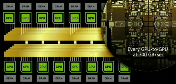
Unlike some of the switches that we see in the HPC arena coming out of China, which are derivatives of InfiniBand switching that are licensed from Mellanox Technologies, the NVSwitch ASIC is a homegrown device that has been under development for the past two years, Ian Buck, vice president and general manager of accelerated computing at Nvidia, tells The Next Platform. The NVSwitch ASIC has over 2 billion transistors, about a tenth of the Volta GPU, and it creates a fully connected, non-blocking crossbar switch using the NVLink protocol, which means every port on the GPUs linked to the switch can talk to all of the other ports (in a point to point manner) at full speed.

The switch chip has a total of 18 ports, which provide 50 GB/sec of bandwidth per port and which, if you do the math, use 25 Gb/sec signaling just like the NVLink ports on the Volta GPU accelerators and the IBM Power9 chips. The NVSwitch has an aggregate of 900 GB/sec of switching bandwidth, and a bunch of the switches can be interconnected and cascades to scale the Tesla network in any number of topologies. The ports on the switch aggregate eight lanes of 25 Gb/sec signaling
 
Last edited:
You think that may be why he is calling it the "worlds largest gpu" due to the new fabric-switch connectivity and non-blocking?
Only reason I can think of and also takes NVLink 2 to another level, also wonder if there will be a comparable Power9 solution down the line.
It seems like the high bandwidth and shared memory space enabled by having NVLink connecting everything is the marketing point. At a device level I'm not sure it's fully transparent.
 
It seems like the high bandwidth and shared memory space enabled by having NVLink connecting everything is the marketing point. At a device level I'm not sure it's fully transparent.
It is meant to be a unified memory space so has to be transparent to minimise overheads I assume <[edit] listened back and he mentions all GPUs using same memory model>
Also needs to be a neat solution for the cache coherency that is supported by Volta.
But your right not much else can be said for now as it is a high level presentation.


Edit:
Past tense to current.
Transparency level to me comes down to the NVLink protocol in the fabric switch (if truly non-blocking crossbar).
 
Last edited:
Memory access latency must surely be pretty rotten, GPUs talking to each other from across a 2 billion transistor switching chip connected by a bunch of (probably fairly long) cables.
 
http://www.tomshardware.com/news/nvidia-turing-graphics-architecture-delayed,36603.html

Tom's says that Ampere is actually Volta successor for the professional field and Turing the gaming architecture. And neither would be unveiled at GDC or GTC.

Turing hasn't yet taped out and is expected back from the fab any day now apparently. Expected launch is late Q3. So the PC gaming market will at least have something for 2018. My Source indicated that next is 7nm Ampere due sometime in H1'19 and that 7nm Gaming GPUs will be delayed given initial 7nm wafer availability and costs.
 
Turing hasn't yet taped out and is expected back from the fab any day now apparently. Expected launch is late Q3.

I’m assuming you meant has taped out if it’s expected to be back any day. tape out to working silicon can be 10-12 weeks with modern finfet processes.

Anyways, this makes me sad, it been almost 2 years since I got my Pascal. I just hope the new boards deliver.
 
Memory access latency must surely be pretty rotten, GPUs talking to each other from across a 2 billion transistor switching chip connected by a bunch of (probably fairly long) cables.
I was wondering myself about latency and was going to post that as well (it will be very low although still there and mostly masked due to what it is used with and what operations) but I am not sure it is something that will truly be made public and only those who know are clients with the DGX-2 or looking at the NVSwitch beyond this in the future.
Reason for the amount of transistors is that a crossbar is pretty inefficient design (number of connections as done by Nvidia) when implemented as non-blocking.
The longer cables outside the NVSwitch best bet is to look at existing NVLink latency with V100 in more normal DGX-1 implementation or maybe Quadro V100 that can do a pair NVLink.

That said we may get more figures on their comparing the DGX-2 to say DGX-1 that very indirectly gives us a consideration if latency is a burden; one example they gave is that it is 10x faster than the DGX-1 I think for a huge training dataset due to the unified memory space and way the NVSwitch connects all the dGPUs - it has double the V100s but the performance difference is vastly more than that and here latency is a non-issue.
Yeah such tests will be carefully chosen :) still probably the best public will see.

Edit:
Regarding latency and BW, possibly the biggest aspect will be the fabric crossbar switch connecting both stacked enclosures (each with 8 GPUs), forgot to mention that aspect.
 
Last edited:
I’m assuming you meant has taped out if it’s expected to be back any day. tape out to working silicon can be 10-12 weeks with modern finfet processes.

Anyways, this makes me sad, it been almost 2 years since I got my Pascal. I just hope the new boards deliver.

Yes that's what I meant. And you are correct, it can take that long. I'm actually quite curious to see how they perform. The fact that NV has finally gone for distinct gaming and compute focused architectures is good for both segments.
 
Memory access latency must surely be pretty rotten, GPUs talking to each other from across a 2 billion transistor switching chip connected by a bunch of (probably fairly long) cables.
Latency is also a secondary concern for parallel architectures. Doesn't seem all that different from what Epyc did with Infinity fabric and situationally it's a superior solution.

Reason for the amount of transistors is that a crossbar is pretty inefficient design (number of connections as done by Nvidia) when implemented as non-blocking.
It probably isn't a crossbar but a mesh fabric like what AMD did with Infinity. Both of those techniques likely came from DoE research with HPC. I'd imagine there is a fair chunk of SRAM on that chip to buffer all the connections that accounts for much of the transistor count. Current Xeons wouldn't have the link bandwidth (but probably could with proprietary signaling) or enough lanes. Perhaps with the upcoming scalable designs. Epyc with IF might work, but I could see that pairing being problematic and a proprietary solution more in Nvidia's interest.
 
It seems like the high bandwidth and shared memory space enabled by having NVLink connecting everything is the marketing point. At a device level I'm not sure it's fully transparent.

The full Volta memory model is supported to all remote GPU memories connected by NVSwitch. You can dereference any pointer, without doing any work in software to figure out where in the system that pointer points. You can use atomics.

It’s not transparent to the GPUs themselves - obviously they have to have page tables that disambiguate the memory reference. But it’s all done in hardware, so from the programmer’s viewpoint it really does look like one memory.
 
Turing hasn't yet taped out and is expected back from the fab any day now apparently. Expected launch is late Q3. So the PC gaming market will at least have something for 2018. My Source indicated that next is 7nm Ampere due sometime in H1'19 and that 7nm Gaming GPUs will be delayed given initial 7nm wafer availability and costs.

Have you heard anything about the process in which Turing is made? Late Q3, some products probably Q4 sounds very late for 12nm. 7nm Products should be possible in Q3 19, which gives the products less than a year life. Could it be maybe 10nm? This way Nvidia could skip the normal 7nm process and directly go to 7nm EUV.
 
Latency is also a secondary concern for parallel architectures. Doesn't seem all that different from what Epyc did with Infinity fabric and situationally it's a superior solution.


It probably isn't a crossbar but a mesh fabric like what AMD did with Infinity. Both of those techniques likely came from DoE research with HPC. I'd imagine there is a fair chunk of SRAM on that chip to buffer all the connections that accounts for much of the transistor count. Current Xeons wouldn't have the link bandwidth (but probably could with proprietary signaling) or enough lanes. Perhaps with the upcoming scalable designs. Epyc with IF might work, but I could see that pairing being problematic and a proprietary solution more in Nvidia's interest.
Not sure Anarchist because Nvidia happily mention when using mesh and everywhere they are calling it a non-blocking crossbar switch (that is the crux it and why I say if in the other posts), along with the transistor count and requirements for a crossbar.
With the limited information so far seems to me it is a different approach to AMD and possibly more similar to another IHV.

Yeah seems Nvidia's appoach was indirectly from DoE and I cannot help think inspired with what IBM does internally with the Power9 fabric switch, that could manage 7TB/s aggregate on chip switch (I need to go back and look at some of the IBM's presentations).
I would be hesitant to say which is superior as there are also aspects to NVSwitch that has advantages but it is for a dedicated and specific purpose.
 
Last edited:
I would be hesitant to say which is superior as there are aspects to NVSwitch that has advantages but it is for a dedicated and specific purpose.
Not saying either is superior, just variations on the same basic idea scaled differently. Both likely have merits for different applications and different requirements for flexibility. IF restricted to PCIe signaling specs with a wider variety of hardware. NVSwitch likely limited to a specific generation of GPU with bandwidth maximized. A mesh is technically still a bunch of crossbars. IBM, Infiniband, etc are all similar network topologies for the most part.

The non-blocking part is interesting as the network will encounter congestion eventually and it only makes sense with exclusive access or significantly over-specced bandwidth. Guessing that's only in reference to cache access on another GPU, not shared memory. Although the switch bandwidth and HBM2 bandwidth are equivalent.

NextPlatform said:
The NVSwitch has an aggregate of 900 GB/sec of switching bandwidth, and a bunch of the switches can be interconnected and cascades to scale the Tesla network in any number of topologies.
To have topologies there will be multiple hops to reach a destination eventually. The result will be some sort of NUMA configuration.
 
Not saying either is superior, just variations on the same basic idea scaled differently. Both likely have merits for different applications and different requirements for flexibility. IF restricted to PCIe signaling specs with a wider variety of hardware. NVSwitch likely limited to a specific generation of GPU with bandwidth maximized. A mesh is technically still a bunch of crossbars. IBM, Infiniband, etc are all similar network topologies for the most part.

The non-blocking part is interesting as the network will encounter congestion eventually and it only makes sense with exclusive access or significantly over-specced bandwidth. Guessing that's only in reference to cache access on another GPU, not shared memory. Although the switch bandwidth and HBM2 bandwidth are equivalent.


To have topologies there will be multiple hops to reach a destination eventually. The result will be some sort of NUMA configuration.
You do not need NUMA or equivalent for a cascade crossbar switch, scaling comes down to how well the NVLink works, along with various other design limitations (such as will be a limit to cascade, still need a CPU:accelerator ratio for optimal performance,BW-connection limitations,etc).
Non-blocking regarding memory consideration you raise would be all aspects of memory that can be associated with current NVLink and Volta architecture, the limitation (more to do with BW-connections-some latency) and where more information is required is how the enclosures are interconnected (still in context of crossbar switch).
Most of this is academic anyway, because the "node" DGX-2 scaled out is enough for quite awhile in current setup and a big jump for the Nvidia performance where it is meant (HPC related analytics-databases-science-modelling-DL).

Just to add, like I mentioned earlier a lot will not be made public so one needs to rely upon actual performance results when compared to DGX-1, such as when they used a massive dataset for training and the DGX-2 was 10x faster (Nvidia will be careful with examples but most would be in line with what the product is for anyway).


Edit:
Expanded upon points.
 
Last edited:
This is the world’s largest GPU which is equivalent to 16 Tesla V100 GB GPU’s connected by 12 latest switch layouts called NVSwitch. These 16 Tesla V100’s each with 32GM of memory creates a virtually 512GB memory. Now, these 512GB of memory in total allows 14TB/sec of aggregate bandwidth which is totally awesome.

For example, If you are having 14000 movies on your computer with each movie having 10GB of space, it will take just 1 second for all those 14000 to get transferred across by NVidia DGX-2. Yes this GPU has 81,920 CUDA Cores and 2 PetaFLOPS to get things done in the blink of an eye.
....
And every signal GPU can make a contact with other GPU without any obstacles because it’s not a network, it’s a switch. Yes, it’s a non-blocking fabric switch, a memory programming module which is exactly the same as inside a chip. The latency of this chip is incredible, unlike a network, this a switch through which each GPU talk with other GPU with low latency.

Screenshot_36.png

http://www.mediatechreviews.com/nvidia-dgx-2-largest-gpu/
 
Nice to see another comparison on their site beyond the massive dataset training performance mentioned in the keynote, closer to more traditional workloads (except IFS benchmark still does not indicate the application).
 
Last edited:
So the reason for 6 NVSwitch per baseboard is the ideal number for ratio with NVLInk GPUs and Volta (6 bricks-ports in a single V100), while also with full non-blocking to other baseboard.
Each NVSwitch on one baseboard seem to have the same control plane with co-ordinated switching fabrics, this allows the 1:1 hop same baseboard while aggregating each GPU across all NVSwitches, with Volta having 6 NVLink bricks (ports) each brick is connected to a single NVSwitch (hence 6 NVSwitches), meaning all GPUs on one baseboard are on all the same NVswitches together at full bandwidth.

The architecture allows each of the individual NVSwitch to combine (possible as the 6 switches already use the same control plane) to link aggregate as a whole meaning 300GB/s to the GPU even though the GPU "lanes" is shared amongst the 6 NVSwitches to a single GPU.
Closest network switch example would be Multi Chassis Link Aggregation, the advantage for Nvidia is that NVLink and Nvidia's associated proprietary protocol/algorithms (such as Exchange/Sort hashing functions) is used all the way through the architecture and internally from GPU device to switch to GPU device; the limitation to scaling like I mentioned earlier would be NVLink, connections (ports), cascade limit/Multi Chassis Link Aggregation equivalent limit.
But Nvidia would realistically stay with a similar topology going forward, and it would have big advantages even for the DGX-1 or any HPC solution with more than 4 GPUs per node (point after split-balanced between NUMA CPUs), trickle down later on makes sense but how much it impacts price also needs to be seen.

With Bisection bandwidth now public, clear it is a true non-blocking crossbar switch design also between the baseboards that house 8 GPUs each and at full BW potential of NVLink.

Edit:
If looking into Multi Chassis Link Aggregation I would be wary in using the wiki explanation as a complete understanding, compounded that it can be highly proprietary in implementation and more so if one has relevant Intellectual Property that is applicable to both device and switch.
 
Last edited:
More public information regarding NVSwitch: https://www.nextplatform.com/2018/04/13/building-bigger-faster-gpu-clusters-using-nvswitches/
What is missing from this is the control plane information that is between the NVSwitches.
Summary is 2 hop same board, 3 hops max any GPU and with the bisection BW of 2.4GHz means pretty clearly 8 lanes-ports per switch connecting to the other baseboard NVSwitch for the non-blocking and low latency/hope count.
One aspect still a consideration is GPU saturation where 1 GPU communicates simultaneously to more GPUs than the number of bricks-ports it has (6), but management of this comes down to Nvidia's NVLink/Unified Memory Space-coherent Unified Memory.

Separately but worth noting elite partners are now pushing out information and looking to take orders for DGX-2.
It will be interesting to see how soon a certified solution based upon the NVSwitch/baseboard is launched, several elite partners are certified to do this in the past with NVLink and Pascal/Volta.
 
Last edited:
Back
Top