
I think no-x posted some 3dmark fillrate numbers a while back that pointed to 32.
Given that the test is for HD 4850 with GDDR3 memory... Is it possitlbe that it got hit by bandwidth limit?
I might be wrong anyway, it is only my assumption.
I think no-x posted some 3dmark fillrate numbers a while back that pointed to 32.
Oh... sorry.Ummm... Isn't Perlin Noise a shader intensive bench?

Originally Posted by Hornet331
Simple mathematics
several fillrate tests from 4850 in the wild show ~19500MT/s and clock of the Card (TMUs) is 625Mhz
with 32TMUs and 625mhz you get a theoretical fillrate of 20.000MT/s
with 40TMUs at 625mhz you get 25.000MT/s.
i dont think RV770 is that inefficent.
The decision to use a two-chip strategy for the high end was made more than two years ago, based on an analysis of yields and scalability. It was not related to AMD's recent financial woes, said Rick Bergman, general manager of AMD's graphics division.
AMD says its 4850 device at about 110 W and $199 will deliver about 75 percent of the performance of Nvidia's high-end GTX280 which costs $649 and dissipates 236W. Two of the AMD parts on a board will hit graphics benchmarks about 30 percent higher than the Nvidia device, the AMD spokesman added.
A 4870 version of the product sporting slightly higher performance will cost $299. Both AMD chips are made in a 55nm process, compared to 65nm for the Nvidia chips, and measure about 16x16mm compared to about 24x24mm for the Nvidia part.
Bergman said the AMD focus on a more mainstream design will enable it to roll out this fall a version for notebook computers that consumes less than 70W. "There's no way this new Nvidia core will be in notebooks this fall," Bergman said.


"I predict our competitor will go down the same path for its next GPU once they see this," Bergman said. "They have made their last monolithic GPU."
Instead it will launch a part aimed at the graphics mainstream with a proprietary interconnect that links two chips on a board to deliver top performance.
Both AMD chips are made in a 55nm process, compared to 65nm for the Nvidia chips, and measure about 16x16mm compared to about 24x24mm for the Nvidia part.
Was the demo developed by Valve?Has AMD aquired VALVe recently? Nonetheless that demo looks really nice, a substantial improvement over the previous ruby demos. I wonder if there is some raytracing involved with that demo, considering those accurate reflections would be very hard to represent with animated textures or other raster techniques, I presume.
It's useful to point out that, in spite of the fact that NVIDIA doesn't support DX10.1 and DX10 offers no caps bits, NVIDIA does enable developers to query their driver on support for a feature. This is how they can support multisample readback and any other DX10.1 feature that they chose to expose in this manner.
"We support Multisample readback, which is about the only dx10.1 feature (some) developers are interested in. If we say what we can't do, ATI will try to have developers do it, which can only harm pc gaming and frustrate gamers."
"The Way It's Meant To Play Dirty" Clearly I'm just being dense here, but what about MSAA readback is a DX10.1 feature? You can read back MSAA samples in DX10. You can't read back a MSAAed depth buffer, but I don't believe you can do that on NVIDIA in DX10 either. What do they mean here when they say they already support DX10.1 "multisample readback"? Are they just mincing words and saying that "hey, we support a feature that was optional in DX10 and required in DX10.1" similar to saying "we already support fp32 filtering" (also option in 10, required in 10.1)?So nVidia can use the "multisample readback"
Found those two quotes in the article somewhat interesting. 256mm sounds about right and a confirmation the interconnect is there. They could be talking about the crossfire link but I'd assume it's something more.
I'm sure those numbers are skewed towards RV770 but they look damn impressive!
http://pc.watch.impress.co.jp/docs/2008/0617/amd_14.jpg
Someone at NVIDIA is crying right now..
And this is a marketing slide, so you can be absolutely sure that the AMD number is rounded down, whereas the nVidia one is rounded up.More interessting on this slide, are the "16 mm", so RV770 is 256mm², like several times said.
Really, until someone goes for the chip with a micrometer, we just won't know the decimals on the 16.xx.Can open it. Is there another way to get to it?
I'm sure those numbers are skewed towards RV770 but they look damn impressive!
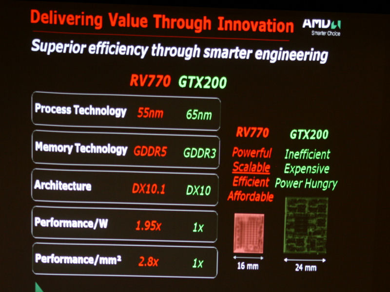
Someone at NVIDIA is crying right now..
