Install the app
How to install the app on iOS
Follow along with the video below to see how to install our site as a web app on your home screen.
Note: This feature may not be available in some browsers.
You are using an out of date browser. It may not display this or other websites correctly.
You should upgrade or use an alternative browser.
You should upgrade or use an alternative browser.
AMD: Pirate Islands (R* 3** series) Speculation/Rumor Thread
- Thread starter iMacmatician
- Start date
-
- Tags
- amd
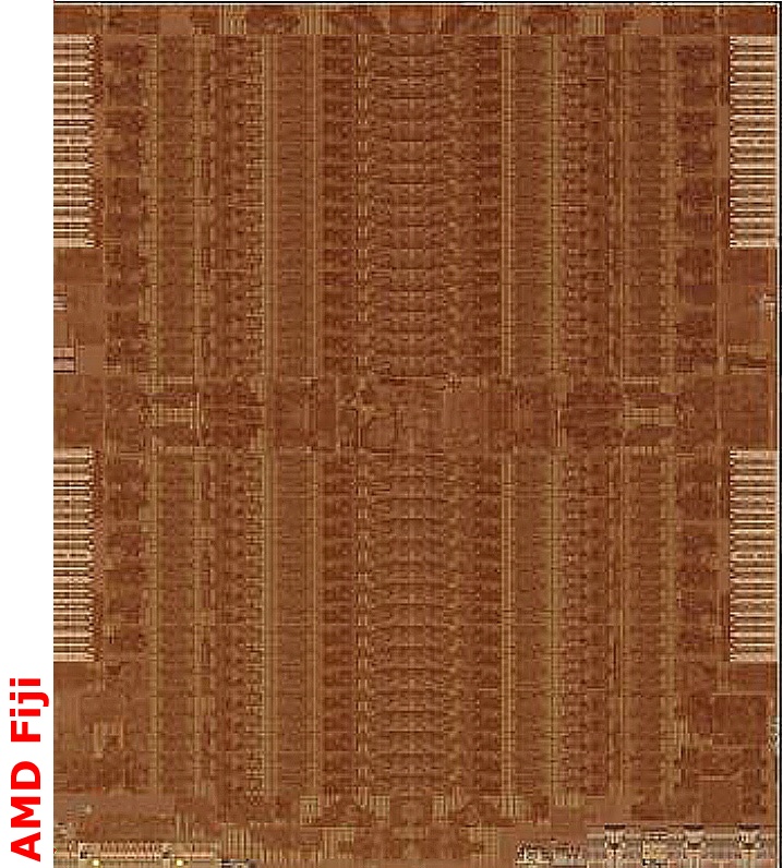
It's a shame that I have to squint that much.
Some rushed pixel counting of what I squinted to be the area of one of the PHY blocks seems to put the area around 5-6% of die area.
That puts it a little past the top end of my guess based on the PHY area given for HBM (24-30mm2 vs 33-36? from pic).
https://forum.beyond3d.com/posts/1844903/
edit: Eh, I picked the side that might have been cropped. It might be 6-7%.
Last edited:
D
Deleted member 13524
Guest
Hawaii's memory interface probably isn't that much "low power". In the 390 series the GDDR5 clocks at 1.5GHz (6GT/s).
Huh? I might remember wrong, but didn't it occupy pretty much 3 of 4 sides of the die?Relative to the rest of the I/O (PCIe, display, etc.) the HBM phy padding looks quite large, but after all this is a ~600 mm² die. The Hawaii's low-power 512-bit interface could probably occupy less area.
I said "probably", since there's no die-shot of Hawaii released, only of Tonga that uses the same phy interfacing.Huh? I might remember wrong, but didn't it occupy pretty much 3 of 4 sides of the die?
The case you're referring is Tahiti, I guess?
Maybe I mixed Hawaii & Tahiti indeedI said "probably", since there's no die-shot of Hawaii released, only of Tonga that uses the same phy interfacing.
The case you're referring is Tahiti, I guess?
Is Hawaii's interfaces really specifically "low power", though? As I recall the way it was described was simply re-purposing tahiti's old, lower-speed memory controllers.The Hawaii's low-power 512-bit interface could probably occupy less area.
Is Hawaii's interfaces really specifically "low power", though? As I recall the way it was described was simply re-purposing tahiti's old, lower-speed memory controllers.
AMD stated Hawaii's 512bit memory interface was 20% smaller in die area than Tahiti's 384bit memory interface, but reference memory speeds dropped from 1500Mhz to 1250Mhz.
D
Deleted member 13524
Guest
AMD stated Hawaii's 512bit memory interface was 20% smaller in die area than Tahiti's 384bit memory interface, but reference memory speeds dropped from 1500Mhz to 1250Mhz.
Again: the speeds went back to 1500MHz in the R9 390 series.
AMD stated Hawaii's 512bit memory interface was 20% smaller in die area than Tahiti's 384bit memory interface, but reference memory speeds dropped from 1500Mhz to 1250Mhz.
If that succession of data points holds, that means Tahiti's ~1/5 of its 365mm2 area devoted to GDDR5 PHY translates to ~73mm2 that translates to ~58mm2.
That seems safely above the guesstimated PHY area of Fiji.

Right, not Tahiti. Like, Cayman, wasn't it? All these codenames are getting difficult to differentiate.AMD stated Hawaii's 512bit memory interface was 20% smaller in die area than Tahiti's 384bit memory interface, but reference memory speeds dropped from 1500Mhz to 1250Mhz.

Well, looks like the HBM phy is just about the same area as the Tonga's 6-channel GDDR5 interface.
That seems to fit the numbers for the succession of interfaces from Tahiti through Hawaii as well.
Tahiti's ~1/5 of its 365mm2 area devoted to GDDR5 PHY translates to ~73mm2 that translates to ~58mm2. 6/8 of that is ~44mm2 which is close to the possibly ~6-7% of Fiji for HBM.
And why did it take more than a year for them to introduce a high volume SKU with all shaders enabled?Why does AMD not enable the full gddr interface on tonga?
That is why it would be nice to have die shots of new revisions as well.Again: the speeds went back to 1500MHz in the R9 390 series.
Probably not worth the increased card complexity. 3 GB would be sweet spot capacity, but nowadays 4 is gonna sell even better.Why does AMD not enable the full gddr interface on tonga?
I'm thinking doing so would put it too close to the R390 in performance.Why does AMD not enable the full gddr interface on tonga?
D
Deleted member 13524
Guest
The difference in performance should be pretty large, since Tonga doesn't clock very high and there's still a big difference in some areas like fillrate.I'm thinking doing so would put it too close to the R390 in performance.
I think it might have to do with the memory capacity options they would have with the 384bit bus (3GB too few, 6GB too much) and PCB complexity.