Install the app
How to install the app on iOS
Follow along with the video below to see how to install our site as a web app on your home screen.
Note: This feature may not be available in some browsers.
You are using an out of date browser. It may not display this or other websites correctly.
You should upgrade or use an alternative browser.
You should upgrade or use an alternative browser.
If GK104 would be such a huge die and with a 384bit bus yes.
If it's supposed to be trading blows with Tahiti, why wouldn't it be?
Because rumors say it's 256bit?
GK104 wants to be measured:
http://www.chiphell.com/forum.php?mod=viewthread&tid=371058&page=7#pid11248448
http://www.chiphell.com/forum.php?mod=viewthread&tid=371058&page=7#pid11248448
GK104 wants to be measured:
http://www.chiphell.com/forum.php?mod=viewthread&tid=371058&page=7#pid11248448
Thanks.
The chip itself looks quite tiny

Direct Link to a mirror:GK104 wants to be measured:
http://www.chiphell.com/forum.php?mod=viewthread&tid=371058&page=7#pid11248448
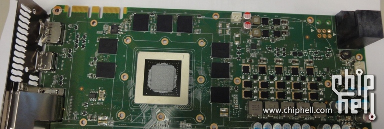
Yes, that's about the number I arrive at, too. The die is slightly larger than twice the size of a memory chip, which measures 12x14=168mm².~356 mm² (?)
Resolution is quite limited, so error can be pretty significant.
Just counting pixels in a amateurish attempt of rectifying the picture, I get ~349mm² (which has indeed a quite high error margin due to the limited resolution). But it probably means that Charlie was not far of with his 18.5x18.5=342mm² die.
Edit: So the "marketing die size" could be about Cypress size, i.e. 330ish.
Last edited by a moderator:
~323,4mm²GK104 wants to be measured:
http://www.chiphell.com/forum.php?mod=viewthread&tid=371058&page=7#pid11248448
Reference length -- the SLi contacts.
Yes, I did.fellix: Did you take perspective into account?
That by itself would enlargen the apparent die size. I would suspect the rounded edges of the connectors as the source of discrepancy. The memory chips and the die have hard edges, which makes it easier to get it right. But it doesn't solve the low resolution problem. I would put at least a 15mm² margin on every number derived from that picture, just by the +/- 1 pixel uncertainty to determine the edge of the chips. As one does it twice, it's actually even larger in the worst case.fellix: Did you take perspective into account? SLI connectors ar more distant than the GPU.
boxleitnerb
Regular
12mm x 14mm
12mm x 14mm
So that would put it at roughly between 337 and 347mm^2 or so
As said above, a GDDR5 BGA170 module measures exactly 12x14=168mm².Quick photochopping tells that the die is roughly 1.33 times (or 1.53 times the height) the width of GDDR5 memory module, and roughly square, so what's the width of GDDR5 module?
Taking your (not perfectly consistent) numbers, you also arrive in the 340ish mm² ballpark.
As said above, a GDDR5 BGA170 module measures exactly 12x14=168mm².
Taking your (not perfectly consistent) numbers, you also arrive in the 340ish mm² ballpark.
Missed it
But anyway, yes, I arrived at around those numbers too, that was on quick photochopping on lowresolution image though, the measuring that is, so there's about 1-2 px thresold in just that, let alone how much the low res affects everything
But aside from that, we can quite safely conclude that it's smaller than Tahiti for sure - has nVidia managed to not only catch but also pass AMD on the perf/mm^2 front, and do it with ~1/3rd the mem bandwidth, or is it safe to say GK104 can't challenge Tahiti outside nVidia handpicked (GPU PhysX) situations?
If it's supposed to be trading blows with Tahiti, why wouldn't it be?
Because rumors say it's 256bit?
Which Tahiti exactly for one and directly after that since when does buswidth by itself define a GPU's performance? What a surprise Cayman had a 256bit bus yet was on average about 15% behind a GF110 with a 384bit bus.
***edit: and just for the "rumor's" sake I count 8 memory chips on that picture above.
Similar threads
- Replies
- 12
- Views
- 2K
- Replies
- 183
- Views
- 18K
- Replies
- 56
- Views
- 7K
- Replies
- 85
- Views
- 11K