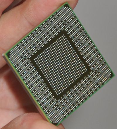
I compare the pictures of G80, GT200 and GF100. And i saw this:
....
I think GF100 has a g80 die size.
Ugh, would you mind detailing the approach you used in your comparison? What did you choose as SR in order to ensure that you're actually comparing comparable things, how do you know the package:die ratio and so on and so forth. I'm certain you took all those precautions to arrive at such a decisive conclusion, no?