
Ok, yes in that case 625/1296 doesn't make sense.
Could be a typo. In any case 1250-1300 hot clock for the 470 sounds within so far expecations.
Ok, yes in that case 625/1296 doesn't make sense.
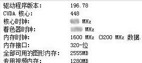
And it seems its showing 1296MHz for shader clock..
Yep, that was precisely why I was questioning your earlier comment about 1Ghz being the lowest bin. Dropping down to 1.35v from 1.5v may result in considerable power savings (and they might be cheaper to boot).
Yes, the savings in power consumption may be significant. Also, the 470 and 480 have a much wider memory interface than HD 58xx, so there is much less need to have GDDR5 mem with ultra high clocks.
Digital circuits have two main building blocks: transistors and wires. Transistors do the switching and store information, but they must be connected with wires.
In general, transistors switch faster as they get smaller. But wires get slower as they get smaller, for two reasons. Firstly, it's just hard to push current through small wires - this is called resistance. Secondly, the wires get packed closer together, which increases capacitance. Roughly speaking, with every new process generation, the transistors get a little faster and the wires get a little slower, and we're now at the point where the wires can dominate the time and power characteristics of a circuit.
You can make a wire propagate a signal faster many ways, here are a few:
1. Move the wire to a bigger metal layer. Generally, the lowest metal layers in the stack are the smallest, and are used for short connections. As you go higher in the metal layer stack, the wires get bigger (but there are fewer of them), which makes for less resistance and capacitance.
2. Cut the wire into pieces. The time it takes a signal to travel through a wire superlinearly related to its length. If you break the distance up into smaller hops, the sum of the delay for the entire path can be quicker. At the end of each hop, the signal has to jump back down to the transistor layer in order to be reboosted back to full strength and sent out to the next hop. This is called "buffering". You can only do this with a metal spin if you have extra buffers lying around which aren't being used - to add new buffers that aren't there would require a full silicon respin.
3. Make the wire shorter. Depending on the flexibility of your design, you can change the physical placement of the transistors it's connecting to make the path shorter. This is hard to do in a metal spin, and often introduces problems of its own: if you make one wire shorter, you often make another wire longer.
")
GTX470:
Vantage P16600
crysis,1920X1200 veryhigh+8x aa,24fps
crysis,1920X1200 veryhigh+No aa,53fps
Rumor from Chinese forum~
http://mylab.q.yesky.com/thread-121-1-1.html

So going on that, and taking THG's benchmarks - http://www.tomshardware.com/reviews/radeon-hd-5970,2474-8.html -
The 470 beats crossfired 5870's without AA, but loses to the 5850 with 8xAA.
This seems a tad unlikely but if true at least we know what kind of benchmarks to expect come March 26th.
Non-public variant of a GF100 SKU
More featured VRM circuity, no sign of vent openings in the PCB, 1xDVI, 1xHDMI and 1xDP on the backplate.
From the M-one non-public version of this screenshot GF100 PCB board point of view, this piece of M-one non-public version of GF100 for 10-layer PCB design, length of about 10.5 INCH, about 266.7mm. 6PIN, and one each in 8PIN external power interface is expected to power more than 360W (very strong). The core power supply 12-phase, output 18 of tantalum capacitor, the input six solid capacitors. 2-phase memory power, output two solid tantalum capacitors and two capacitors, two solid-state input. Interface portion of DP + HDMI + DVI + VGA 4 interface design. Judging from DX 11 areas of ATI "lonely" days coming to an end

How do you figure that?The IHS has the same size like the G80 one. So, a die size over 529mm^2 is wrong.
How do you figure that?

The die is under that IHS in all cases. As in, it's not that size, and you can't tell just by looking at it.I think GF100 has a g80 die size.