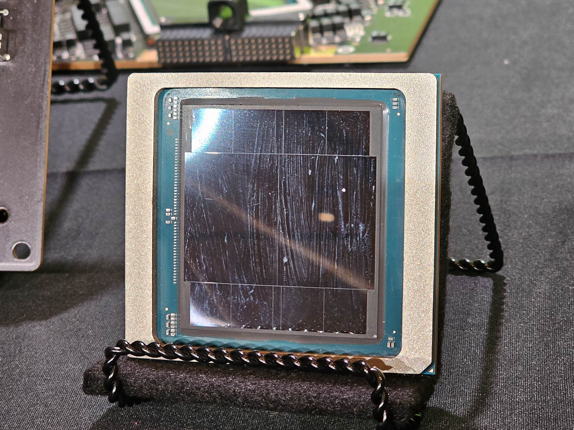
At least in hardware they do, it's 2 identical (or mirrored) chipsYeah kinda strange. NextPlatform mentioned something about an architecture briefing. Did that happen?
Similar to MI300X I’m curious to understand how work is submitted to B1/200. Does each die have its own set of schedulers and the host runtime divvies up the work accordingly?
Install the app
How to install the app on iOS
Follow along with the video below to see how to install our site as a web app on your home screen.
Note: This feature may not be available in some browsers.
You are using an out of date browser. It may not display this or other websites correctly.
You should upgrade or use an alternative browser.
You should upgrade or use an alternative browser.
Artist render is showing identical chips, just rotated to mate.At least in hardware they do, it's 2 identical (or mirrored) chips
Can't think of any benefits of doing a mirrored chip for aligning a single full side.
IMO it would just added unneccessary complexity and extra steps but maybe I'm missing something.
The render also shows what appears to be two alignment tabs and almost looks like the interconnect is coming off/overhanging the edge of the die.... so YMMV.
Edit- Added the other image from anandtech.
Dang you're fast Kaotik, caught me in the middle of an edit. LoL
Attachments
Last edited:
Artist render is one thing, but NVIDIA stated it's 2x10⁴B transistor chips so it doesn't really leave room for anything but identical chipsArtist render is showing identical chips, just rotated to mate.
Though it also shows what appears to be two alignment tabs and almost looks like the interconnect is coming off/overhanging the edge of the die.... so YMMV.
TopSpoiler
Regular
Artist render is one thing, but NVIDIA stated it's 2x10⁴B transistor chips so it doesn't really leave room for anything but identical chips
Yeah I assume it’s two identical chips with one rotated 180° to mate.
Fun fact: 7 years ago NV researchers put 6TB/s inter-GPU bandwidth to the 'unbuildable' category. Now Blackwell has freaking 10TB/s.
Monoliths have also gotten bigger and faster in those 7 years. The inter-chip bandwidth to match an equivalent unbuildable monolith today could very well be north of 10TB/s.
Graphics scheduling is harder than compute scheduling.
neckthrough
Regular
Could you ELI5 why?Graphics scheduling is harder than compute scheduling.
Is it a fundamental algorithmic issue? Or an artifact of the current HW/SW interface?
Could you ELI5 why?
Is it a fundamental algorithmic issue? Or an artifact of the current HW/SW interface?
This is how I ELI5 to myself.
Compute workloads are pretty uniform. e.g. need to execute 5,000,000 instances of the same program. So relatively trivial to distribute work uniformly across multiple SMs/GPCs/GPUs/nodes/racks.
Graphics queues and command lists are a whole different story with tons of varied workloads in terms of size, data payloads, dependencies, runtime etc. Today the orchestration of all this graphics work is done by a central scheduler on-chip. Efficiently allocating work across multiple schedulers & chips is a much tougher problem.
It's sorta spelled out in the Nvidia paper too.
In this paper we propose the MCM-GPU as a collection of GPMs that share resources and are presented to software and programmers as a single monolithic GPU. Pooled hardware resources, and shared I/O are concentrated in a shared on-package module (the SYS + I/O module shown in Figure 1). The goal for this MCM-GPU is to provide the same performance characteristics as a single (unmanu- facturable) monolithic die. By doing so, the operating system and programmers are isolated from the fact that a single logical GPU may now be several GPMs working in conjunction. There are two key advantages to this organization. First, it enables resource sharing of underutilized structures within a single GPU and eliminates hard- ware replication among GPMs. Second, applications will be able to transparently leverage bigger and more capable GPUs, without any additional programming effort.
Alternatively, on-package GPMs could be organized as multiple fully functional and autonomous GPUs with very high speed in- terconnects. However, we do not propose this approach due to its drawbacks and inefficient use of resources. For example, if imple- mented as multiple GPUs, splitting the off-package I/O bandwidth across GPMs may hurt overall bandwidth utilization. Other com- mon architectural components such as virtual memory management, DMA engines, and hardware context management would also be pri- vate rather than pooled resources. Moreover, operating systems and programmers would have to be aware of potential load imbalance and data partitioning between tasks running on such an MCM-GPU that is organized as multiple independent GPUs in a single package.
DegustatoR
Legend
The best solution to that problem is to have extra-chiplets communication at speeds similar to that of intra-chip communications at which point you can just use one of the global schedulers to distribute work to all of the chiplets.
Which is also why I have doubts that graphics will ever scale well to >1 chip as having the above seems highly unlikely to happen any time soon.
Which is also why I have doubts that graphics will ever scale well to >1 chip as having the above seems highly unlikely to happen any time soon.
The best solution to that problem is to have extra-chiplets communication at speeds similar to that of intra-chip communications at which point you can just use one of the global schedulers to distribute work to all of the chiplets.
Which is also why I have doubts that graphics will ever scale well to >1 chip as having the above seems highly unlikely to happen any time soon.
My vote would be for the solution proposed in the paper. Single scheduler chipset that faces the host CPU + bunch of worker chiplets that receive work from the scheduler over a fast interconnect. Maybe it'll be ok to disable one of the schedulers in a 2 chip setup. But once it extends to 4/6/8 chiplets that becomes very wasteful.
Last edited:
To process these datasets efficiently on GPUs, the Blackwell architecture introduces a hardware decompression engine that can natively decompress compressed data at scale and speed up analytics pipelines end-to-end. The decompression engine natively supports decompressing data compressed using LZ4, Deflate, and Snappy compression formats.

NVIDIA GB200 NVL72 Delivers Trillion-Parameter LLM Training and Real-Time Inference | NVIDIA Technical Blog
What is the interest in trillion-parameter models? We know many of the use cases today and interest is growing due to the promise of an increased capacity for: The benefits are great…
Maybe nVidia will update the decompression engine for DirectStorage.
TopSpoiler
Regular

【笠原一輝のユビキタス情報局】 AI特化設計になったNVIDIA Blackwell、並列性を向上する仕組みが強化
NVIDIAは3月18日~3月20日(米国時間)の3日間に渡り、同社のAIやデータセンター向け半導体などに関する話題を扱うフラグシップ年次イベント「GTC」を、米国カリフォルニア州サンノゼのサンノゼコンベンションセンターにおいて開催した。基調講演の中で、新しいAI/データセンター向けGPUアーキテクチャ「Blackwell」が発表され、その最初の製品として「NVIDIA B200 Tensor Core GPU」(以下B200)、「NVIDIA GB200 Superchip」(以下GB200)の2つを今年(2024年)中に投入する計画を明らかにした。
(translated) According to Jonah Alben, Senior Vice President (SVP), NVIDIA GPU Architect, "Blackwell's microarchitecture is completely different from Hopper, but we can't talk about the details at this time," explaining that Blackwell uses a completely different microarchitecture than Hopper.
DegustatoR
Legend
This was known / expected. I wonder if they'll avoid saying anything about non-tensor side of Blackwell even in the whitepaper.
We therefore decided to use LZ4 which, I think, is very, very fast on the CPU.

The big Horizon Forbidden West PC tech interview with Nixxes and Guerrilla Games
Alex Battaglia interviews the development staff at Nixxes to see how they ported Horizon Forbidden West from PS5 to PC in the Complete Edition.
So, i guess the decompression engine will be in gaming Blackwell, too.

The big Horizon Forbidden West PC tech interview with Nixxes and Guerrilla Games
Alex Battaglia interviews the development staff at Nixxes to see how they ported Horizon Forbidden West from PS5 to PC in the Complete Edition.www.eurogamer.net
So, i guess the decompression engine will be in gaming Blackwell, too.
Definitely a very interesting proposition. I assume a game would still need to specifically target the hardware decoder though and then there's the whole question if how the data gets transferred to the GPU in the first place. I'd say this would need to be supported as part of the Direct Storage standard to have any hope of being used widely.
D
Deleted member 2197
Guest
Gaming Blackwell speculation ...
DegustatoR
Legend
Not necessarily. The h/w can just map the DS API calls wherever it wants. But I wouldn't expect a dedicated h/w here as it's not a task which require one.I assume a game would still need to specifically target the hardware decoder though
At what power? 450W like the 4090 or like 700W?Gaming Blackwell speculation ...
DegustatoR
Legend
Why would it be 700W if GB100 is about 2x perf/watt to GH100 and RDNA4 won't have anything for the top end?At what power? 450W like the 4090 or like 700W?
D
Deleted member 2197
Guest
Not sure. Supposedly the power can be tuned within a specific ranges so imagine it would be somewhere between 450W and 700w.At what power? 450W like the 4090 or like 700W?
All depends on the performance target.
Not necessarily. The h/w can just map the DS API calls wherever it wants. But I wouldn't expect a dedicated h/w here as it's not a task which require one.
So you're saying that if a game uses LZ4 via DirectStorage for CPU decompression as standard (like Forbidden West does) then the HW could automatically move the decompression off the CPU on to the hardware based decoder?
If true then that would make this a lot more usable.
I disagree there's no need for it though (or at least no benefit to be had from it) as it's clearly going to reduce CPU load in games that use LZ4 on the CPU for streaming. I guess it could also potentially be faster than the CPU for the big initial loads.
This was obviously the hope for Gdeflate but so far it's not working out as intended it seems.


