
You are using an out of date browser. It may not display this or other websites correctly.
You should upgrade or use an alternative browser.
You should upgrade or use an alternative browser.
NVIDIA GT200 Rumours & Speculation Thread
- Thread starter Arun
- Start date
- Status
- Not open for further replies.
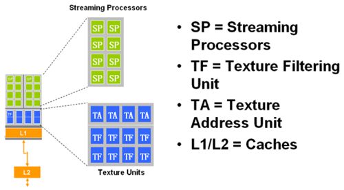
SM = Shader Multiprocessor
RF = Register File
OK. Thanks!
")
Right, that's why I said per SM, rather than per cluster
Uhm but 2x8x10 equals to 160... This simply does not add up with the 240 figure...
So in each cluster there should be other 8 SP that are not counted in the SM?
Uhm but 2x8x10 equals to 160... This simply does not add up with the 240 figure...
So in each cluster there should be other 8 SP that are not counted in the SM?
Like Rys said the changes are at the SM level. Doesn't have anything do with the number of SM's per cluster (could still be 3 for a total of 240 SPs)
The 8 SP you're referring to is an SM.
Like Rys said the changes are at the SM level. Doesn't have anything do with the number of SM's per cluster (could still be 3 for a total of 240 SPs)
The 8 SP you're referring to is an SM.
OK, so it could be the inclusion of a scheduler and RF for each SM (instead of one for each cluster), leaving each SM completely independent form others in terms of thread processing? :smile:

OK, so it could be the inclusion of a scheduler and RF for each SM (instead of one for each cluster), leaving each SM completely independent form others in terms of thread processing? :smile:
Each SM already has its own scheduler and RF in G80 AFAIK. When it comes to CUDA all considerations are always per SM - registers, threads, shared memory etc. It looks like the only things the SM's share are the TMUs and L1 cache and are independent otherwise.
Edit: Heh, pretty much just like that ^
So mystery solved, I suppose...
But what does IU mean, in your opinion? And what's that "local memory"? Maybe they have embedded the L2 cache into each SM?
I still ask me, if on GT2xx MUL is fully enabled for general shading tasks, which units will do the interpolations and tasks, which did MUL on G8x/G9x?
Or are they going MADD+MUL+MUL?
btw.
GTX 280 runs Crysis 1920x1200 VH ~ 34FPS Avg?
Or are they going MADD+MUL+MUL?
btw.
GTX 280 runs Crysis 1920x1200 VH ~ 34FPS Avg?
Last edited by a moderator:
nVidia slides from CJ clearly show that in official numbers it's 240. Of course, perhaps they really will be more powerful due to the "rediscovered MUL".And while I'm at it, I don't think it's 240 either
Not quite solvedSo mystery solved, I suppose...
But what does IU mean, in your opinion? And what's that "local memory"? Maybe they have embedded the L2 cache into each SM?
Those resources (scheduler and RF) have been per-SM from the beginning, and their basic architecture doesn't really change with this new chip (although RF is a different size now).L2 is pooled still (but bigger proportionally, there's quite a lot of SRAM on this thing, although nothing compared to RV770
).Yeah, I said upstream that it's 240 FP32 SPs.nVidia slides from CJ clearly show that in official numbers it's 240. Of course, perhaps they really will be more powerful due to the "rediscovered MUL".
GTX280 CRYSIS 1920*1200 VH Average FPS Reached to 36.81!
GTX280 CRYSIS 1920*1200 VH Average FPS Reached to 36.81!
2008-6-9 16:10:43
Japan IT Media website today brings us the CRYSIS 1920*1200 VH test result of NVIDIA next generation flagship -GeForce GTX 280 Graphics Card.
According to IT Media said, NVIDIA and an anonymous motherboard manufacturer hold a secret presentation to show the performance of GTX 280 outside the Computex 2008.
The visitors said that the demonstration room is very dim lighting. In addition to show the performance of GTX 280 graphics card, the secret presentation also shown parts of the motherboards which are compatible with GTX 280, they simply had been placed on the windowsill of the room.
IT Media site had the opportunity to run GPU-Z, CPU-Z and Crysis Benchmark on the GTX 280 demo system. From the photos, we can clearly see that NVIDIA GTX 280 presentation system used Intel Core 2 Quad four-core processor, the frequency is 2.66GHz, the Crysis Benchmark with 1920 x1200 VeryHigh settings indicated that the average fps of GTX 280 graphics card reached 36.81!
source
http://www.pczilla.net/en/post/35.html
Ouchie on the possible price!G200-A3 with GDDR5 as $899 Ultra-like product?
I'd guess a repeat of the Ultra's release. Those that get Rolex dog collars buying a few, then mortals buying in once lack of demand forces price drops.
Not quite solved
L2 is pooled still (but bigger proportionally, there's quite a lot of SRAM on this thing, although nothing compared to RV770
But if we compare that picture with the old SM structure the IU unit and local memory are missing...
And what about RV770, are you thinking of a further increase of cache compared to R600/RV670?
Some people under NDA are hinting Nvidia has even faster products than the GTX 280 (65 nm) on it's schedule for 2008, and it's not the GT200b. Any info on that?
There'll be a "1Tflop+" GT200-based product (with GDDR3) released this quarter, methinks.
That picture's not really representative.
And what about RV770, are you thinking of a further increase of cache compared to R600/RV670?

- Status
- Not open for further replies.
Similar threads
- Replies
- 124
- Views
- 30K
- Replies
- 1K
- Views
- 231K
- Replies
- 64
- Views
- 11K
- Locked
- Replies
- 780
- Views
- 133K