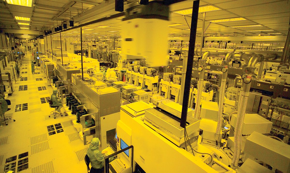
TSMC Execution [2024]

When did they start saying each fab would be doing 100k wafers a month? And 6 giga-fabs in Arizona doing 600k wafers a month? For only $40b? That doesn't sound right.

The original plan was a single fab doing 20k 5nm wafers a month. That number supposedly got upped a bit when they were pressed for additional investment, ~40-50k wafers a month.
I just read a dozen different articles and most appear to be saying that with TSMC's additonal investment of upto $40b, they are expecting 600k wafers per year.

I do quite like other aspects of Hilbert's article though. Not sure where he got the 6 giga-fabs and 600k wafers a month though, those numbers aren't in the source article.

Screw TSMC for still complaining about the increased manufacturing costs after all the subsidies the US and AZ have given them.
Also them trying to boost H1B numbers because there aren't enough "trained/experienced employees." AZ has a shitload of current and ex-semiconductor employees.
If you want robot humans that can follow a set list of steps, I'm sure Taiwan, Thailand, Philippines, Malaysia would be better suited for the low-wage/entry level jobs.
If the role requires any education, adaptability, critical thinking, problem-solving, that just doesn't happen at $100USD per 12hour shift.
 
Last edited by a moderator:
When did they start saying each fab would be doing 100k wafers a month? And 6 giga-fabs in Arizona doing 600k wafers a month? For only $40b? That doesn't sound right.

The original plan was a single fab doing 20k 5nm wafers a month. That number supposedly got upped a bit when they were pressed for additional investment, ~40-50k wafers a month.
I just read a dozen different articles and most appear to be saying that with TSMC's additonal investment of upto $40b, they are expecting 600k wafers per year.

I do quite like other aspects of Hilbert's article though. FJB. Not sure where he got the 6 giga-fabs and 600k wafers a month though, those numbers aren't in the source article.

Screw TSMC for still complaining about the increased manufacturing costs after all the subsidies the US and AZ have given them.
Also them trying to boost H1B numbers because there aren't enough "trained/experienced employees." AZ has a shitload of current and ex-semiconductor employees.
I believe it's suppose to be 600k a year once the second fab comes online. Funny though the Guru3D article mentions eventually 6 fabs running.

The second fab at TSMC's Arizona site (or the second phase of the Fab 21, depending on how you want to look at it) is set to come online in 2026. It will process wafers using TSMC's N3 process technologies, 3nm class nodes that include N3, N3E, N3P, N3S, and N3X. It will also increase production capacity of the camp to 600,000 wafer starts per year, the company announced on Tuesday. It will come online in 2026 and will be one of the foundry's most advanced fabs outside of Taiwan.
 
It also mentions "Vice President Joe Biden" visiting next month [my emphasis], so it has that whole accuracy pedigree pretty much nailed.
Yeah. They have another crew doing these articles and guess it was not proofed before publishing. :whistle:
 
Interesting.... according to the chart, it would actually be very slightly more cost efficient to use a bigger die on 7/6 nm in order to target the same performance vs 5/4 nm (and this includes the efficiency advantage of the smaller node as well). Of course, for the absolute top end, one can't do this due to die size limits; however it could have been an interesting choice for for the smaller, value oriented dies.
 
Interesting.... according to the chart, it would actually be very slightly more cost efficient to use a bigger die on 7/6 nm in order to target the same performance vs 5/4 nm (and this includes the efficiency advantage of the smaller node as well). Of course, for the absolute top end, one can't do this due to die size limits; however it could have been an interesting choice for for the smaller, value oriented dies.
Navi 33 is supposedly N6 monolith
 
Personally I think they should keep building on 7nm to keep costs down the continue releasing the same level of hardware over 4-5 years. It slowly raises the average hardware developers can target on PC so we still get better and better games.

Work on software enhancements like RT, upscale reconstruction, frame generation etc to continue increasing technology stack still.

Of course there's this incumbent craziness that we absolutely must release new faster and better products regularly. Investors and consumerism etc. So it would never stand.
 

Apparently N3 is too expensive even for small(ish) mobile SoC vendors.
 

Apparently N3 is too expensive even for small(ish) mobile SoC vendors.
Small(ish) mobile SoC vendors? Those two command around 65-70% of mobile SoC market and are both in top 5 of ic design companies by revenue (with Qualcomm being the first by huge margin)
 
An interesting note that another commenter picked up on.


The high price of new nodes is driving more business back to older nodes. Those nodes are also more profitable for TSMC which helps them maintain high margins.

Regards,
SB
I don't think it is "driving more business back to older nodes" but I guess it depends on what business we are discussing.
Do we think most of the increased revenue is from current designs of long-term customers needing increased supply on "older nodes" or new designs and/or customers being implemented on "older nodes".
I agree that newer nodes having higher upfront costs and potentially limited ROI, even without the price increases, are a big variable. On the other hand, most businesses today tend to be more cost-conscious and are reluctant to make a change unless 100% necessary.

You also need to take into account, that from the middle of 2020 until the middle of 2022, customers were fighting for every extra wafer they could get from the fabs. The price increases were intended to cover the extra costs of moving to near 100% capacity and allowing those who actually needed it to maybe get some extra wafer starts while also implementing no-cancellation clauses to all future bookings to try and limit double bookings.

28nm, being the last planar node, has the potential for more future revenue records.

Edit- Ugh, hard to get the wording right to create a good flow. My mind is just jumping around. Not sure if I'm making sense.
 
Last edited:
So no die shrink for the consoles?
Slim models are still on the cards, I think. The jump from 7nm to 5nm pricing isn't insignificant, but it's not so painful that the cost reductions in other areas that are gained from a die shrink wont make up for it. Remember, this will allow them to minimize cooling solutions, minimize motherboard costs, use a cheaper PSU, and minimize overall form factor which also importantly helps them reduce product packaging size which reduces distribution costs and warehousing footprint. They also get a lot more chips per wafer, which offers them lower wafer quantities for the same output. Not to mention, that on the PS5 at least, they'll probably update to a more efficient and cheaper SSD setup than its current fairly excessive 12 channel design.

What I wouldn't expect this time around though is any great price reduction. I think MS/Sony would see it more as an opportunity to make their consoles more appealing while at the same time offering better margins for themselves rather than passing much savings to consumers. Though we'll have to see what sales are like by then. For the moment, PS5 and Xbox Series consoles sales dont seem to showing any signs of slowing down.
 
Back
Top