Panajev2001a
Veteran
Are you saying that Nagasaki #2 65 nm lines are for advanced EE+GS production ?
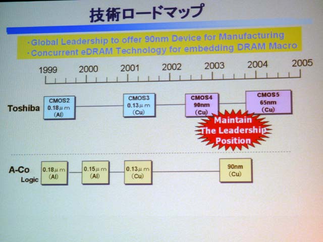
BTW, Nagasaki #2 will ahve the second floor with CMOS4, 90 nm, as that is the process used by the EE+GS@90 nm and PSP.
Few more things:
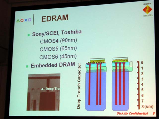
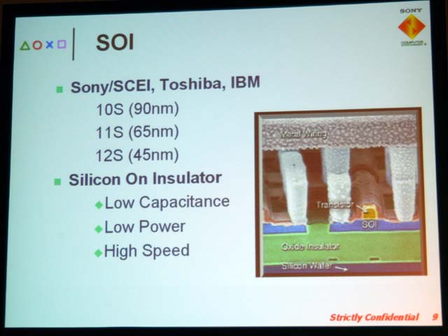
The 65 nm manufacturing process seems to be SOI based... is this CMOS5 ? Is this S11 ( 65 nm IIRC ) ?
When they talk about the investment for Nagasaki #2 they have pictures in their PDFs showing the first floor to be used for CELL production at 65 nm and in that pdf I gave the link in the last post they seemed to associate the two ( I ahve to find a better PDF for Nagasaki #2 ).
BTW, Nagasaki #2 will ahve the second floor with CMOS4, 90 nm, as that is the process used by the EE+GS@90 nm and PSP.
Few more things:
Sony Computer Entertainment and Sony Invest 200 Billion Yen Over Three Years in Semiconductor Fabrication
Installation of fabrication line supporting 65 nanometer process technology
TOKYO, JAPAN, April 21, 2003 - Sony Computer Entertainment Inc. (SCEI) and Sony Corporation (Sony) announced today that they would invest a total of approximately 200 billion yen over three fiscal years from 2003 to 2005 in the installation of a semiconductor fabrication line to build chips with 65 nanometer process on 300 mm wafers.
With this investment, SCEI will manufacture the new microprocessor for the broadband era, code-named "Cell", as well as other system LSIs, to be used for the next generation computer entertainment system. This investment serves an important role not only for SCEI but also for the Sony Group to develop future broadband network businesses.
Of the 200 billion yen, 73 billion yen will be invested in the FY2003. Installment of a new semiconductor fabrication line for building chips with 65 nanometer process on 300mm wafers will be initiated in SCEI's Fab2, a semiconductor fabrication facility located in Isahaya City, Nagasaki Prefecture. Test production will begin using the new fabrication line, gradually moving on to mass production. Execution of the entire investment will be determined by taking optimal timing, place and allocation into consideration.
Since the spring of 2001, SCEI has been engaged, together with IBM Corporation (IBM) and Toshiba Corporation (Toshiba), in the development of the new microprocessor for the broadband era. Also, since the spring of 2002, Sony has participated in the said three company alliance for the development of the advanced semiconductor process technologies. Research and development of digital signal processing technologies for broadband applications are also being conducted.
By means of this investment, SCEI and Sony aim to effectively conduct test production, and to quickly establish a mass production system with 65 nanometer embedded DRAM process.
"Our work with SCEI and Toshiba on the Cell broadband processor has progressed extremely well," said Dr. John Kelly, senior vice president and group executive for the IBM Technology Group. "We believe the Cell design, and the advanced technologies like SOI with which it will be manufactured, will help change the way people work, play and communicate. This announcement by SCEI/Sony is a confirmation of the progress we've made with the Cell design itself, of our advances in semiconductor technology to help it reach its full potential and of Cell's far-reaching implications for a wide variety of applications."
"One of our key semiconductor business strategies is to place Toshiba in the vanguard in providing processor-centric system-on-chip solutions. Cell, which we are developing with SCEI and IBM, is an essential, next-generation broadband processor, a core product whose sales we will actively promote," said Takeshi Nakagawa, Corporate Senior Vice President of Toshiba Corporation. "We expect to apply Cell to a wide range of applications related to broadband networks, including digital consumer electronics and mobile terminals. Today's announcement by Sony group shows that the Cell development project is proceeding as planned and will accelerate the realization of our expectations."
"The introduction of advanced semiconductor technologies is imperative for the next generation processors that support the broadband network era," said Ken Kutaragi, president and CEO of Sony Computer Entertainment and executive deputy president of Sony Corporation. "Digital consumer electronics and network products to enjoy various broadband applications in homes, such as games, movies, music and digital broadcasting, will play a leading role in the future together with the evolution of PC. Sony Group aims to further develop and expand the market with its advanced semiconductor technologies and a rich and wide array of applications. This investment forms a strategic foundation towards this goal."
"SCEI's Fab 2 already applies the most advanced semiconductor technology to produce high performance LSIs, not only for game hardware but also other electronic products," said Kunitake Ando, President and Group COO, Sony Corporation. "The planned investment will further enhance this advanced semiconductor facility to become a technology driver for the next generation of Sony products. Building on this, Sony's Broadband Network Company, newly established as of April this year, will play a key role in developing next generation electronic devices and linkages to game devices."
SCEI and Sony aim to actively develop businesses as leading companies in the broadband network era and to be the driving forces in the next generation semiconductor business.
About Sony Computer Entertainment Inc.
Recognized as the global leader and company responsible for the progression of consumer-based computer entertainment, Sony Computer Entertainment Inc. (SCEI) manufacturers, distributes and markets the PlayStation(R) game console and PlayStation(R)2 computer entertainment system. SCEI, along with its subsidiary divisions Sony Computer Entertainment America Inc., Sony Computer Entertainment Europe Ltd. and Sony Computer Entertainment Korea Inc., develops, publishes, markets and distributes software, and manages the third party licensing programs for these two platforms in the respective markets worldwide. Headquartered in Tokyo, Japan, Sony Computer Entertainment Inc. is an independent business unit of the Sony Group.
About Sony
Sony Corporation is a leading manufacturer of audio, video, game, communications and information technology products for the consumer and professional markets. With its music, pictures, computer entertainment and on-line businesses, Sony is uniquely positioned to be a leading personal broadband entertainment company in the world. Sony recorded consolidated annual sales of nearly $57 billion for the fiscal year ended March 31, 2002. Sony's Home Page
URL:www.sony.net/
The 65 nm manufacturing process seems to be SOI based... is this CMOS5 ? Is this S11 ( 65 nm IIRC ) ?
When they talk about the investment for Nagasaki #2 they have pictures in their PDFs showing the first floor to be used for CELL production at 65 nm and in that pdf I gave the link in the last post they seemed to associate the two ( I ahve to find a better PDF for Nagasaki #2 ).