Tech Power Up's article on the 9600 "Dirty Trick"

http://www.anandtech.com/cpuchipsets/showdoc.aspx?i=3192&p=3
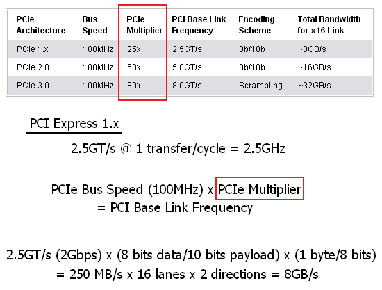
Multipliers.png

the bus speed of pcie 1.x , 2.x and 3.x all are 100mhz not 125mhz.

there is no more "link boost" in 6xx/7xx series chipset mainboard AFAIK, but the GPU Ex is exist that was set to disabled by default. the GPU Ex allow some driver-level optimizations as it requires a 90-series driver.

Yes however, their is no mention of the bus speed when a 2.0 video card is installed.

For example
This modular approach is what allowed the fundamental change in the physical layer data rate from 2.5GT/s to 5.0GT/s to go unnoticed by the upper layers. The PCI-E bus speed remains unchanged at 100MHz; the only feature that changed is the rate at which data is transferred across the board. This suggests that there is significant signal manipulation required on both the transmit and receive ends of the pipe before data is available for use.

There is no mention of what happens when a PCIe 2.0 video card is used and no further explanation as to why/how there is a change in the data transfer.

Futhermore:

As we mentioned before, installing a PCI Express 1.x card in a PCI Express 2.0 compliant slot will result in PCI Express 1.x speeds. The same goes for installing a PCI Express 2.0 card in a PCI Express 1.x compliant slot. In every case, the system will operate at the lowest common speed with the understanding that all PCI-E 2.0 devices must be engineered with the ability to run at legacy PCI-E 1.x speeds.
There is no mention of what the PCIe Freq is when a PCIe 2.0 card is used.


However, if you read the Tech Report
So why is Nvidia using the nForce 200? I suspect it's because the nForce 780i SLI SPP isn't really a new chip at all. Nvidia MCP General Manager Drew Henry told us the 780i SLI SPP is an "optimized version of a chip we've used before," suggesting that it's really a relabeled nForce 680i SLI SPP.

If you recall the last couple of Nvidia SPP chips, you'll remember a feature called LinkBoost, which cranked up the link speed for the chipset's PCI Express lanes... I think we're seeing an extreme version of LinkBoost in action here, with the 780i SPP simply being a 680i SPP whose 16-lane PCIe 1.1 link has been coaxed into running at 4.5GT/s and validated at that speed.
 
Last edited by a moderator:
here is the default bios setting of asus striker ii formula :

biossetting_by_default.jpg


and under this setting, the 9600GT's core clocking is 650MHz that was detected by the RT 2.07 Test 5 version( the 9600GT was installed on the blue PCIE slot that is PCIE 2.0 ):

780i_pcie_2_slot_9600gt_all_default.png


if the PCIE bus clock will change after the 2.0 card installed, the 9600gt core clock should change too here, but that is not happen .
 
here is the default bios setting of asus striker ii formula :
...
and under this setting, the 9600GT's core clocking is 650MHz that was detected by the RT 2.07 Test 5 version( the 9600GT was installed on the blue PCIE slot that is PCIE 2.0 ):
...
if the PCIE bus clock will change after the 2.0 card installed, the 9600gt core clock should change too here, but that is not happen .

You're not supposed to see any changes either in RT or in ForceWare and the following posting clearly explains why:

http://forums.guru3d.com/showpost.php?p=2618787&postcount=3

And honestly I deeply regret about puttting results of our 9600GT clocking investigations in the forum in that thread and allowing it to get into other reviews and news.
That gave me nothing but headache and a lot of users misunderstanding the things and blaming RT for "incorrect" monitoring of 9600. Won't ever publicly share results of my investigations.
 
i understood what you mean, Alex .


there is indeed some people was been misunderstading this info .
 
here is the default bios setting of asus striker ii formula :

biossetting_by_default.jpg


and under this setting, the 9600GT's core clocking is 650MHz that was detected by the RT 2.07 Test 5 version( the 9600GT was installed on the blue PCIE slot that is PCIE 2.0 ):

780i_pcie_2_slot_9600gt_all_default.png


if the PCIE bus clock will change after the 2.0 card installed, the 9600gt core clock should change too here, but that is not happen .


Thanks for the pics, it looks like it maybe board specific. ViperJohn has a Evga 780i and states his is at 125MHz according to clockgen (which reads 124.7). Posted here

...The middle 16x PCIe 1.0x slot is 100Mhz default and is adjustable in system bios. The top and bottom 16x PCIe 2.0 slots are 125Mhz and not adjustable.

Let me clarify this a little more. The PCIe 1.x slots coming off the MCP are running a normal 100Mhz...

So, according to this what's being read in the bios is PCIe 1.X slots coming off the MCP not the PCIe 2.0 slots.

Side note:
Any reason why "enabled driver level hardware overclocking" isn't checked? Do you mind enabling it just to see what happens?

Also

Could you use clockgen?
 
Last edited by a moderator:
So what exactly happened to the LinkBoost feature in the nForce 590 and 680 chipsets anyway? Lots of boards were shipped in that feature and I'm sure NVIDIA couldn't magically disable it just by clapping their hands, so what happened to it? Maybe boards are still out there with LinkBoost working, and they just happened to make it to test beds? Its entirely possible that NVIDIA cards are still being "boosted"....

Speaking of investigative journalism, I discovered something about Max Payne 1 which might have made an article back in say 2002 or so. But, too little, too late I guess.....:(
 
Thanks for the pics, it looks like it maybe board specific.

The EVGA and XFX boards are rebadged boards made to an nvidia specification ( Flextronics, PC Partner, Foxconn?) whereas the Asus is not, so might explain the 2 results.

If it is the case that the reviewers used the EVGA or XFX and it does behave this way then I'm surprised the reviewers do not check the actual clock they are testing at using something like Rivatuner monitor screen. They should be doing this anyway, especially now there are so many overclocked parts on the market to check the validiation of those claimed speeds!
 
Thanks for the pics, it looks like it maybe board specific. ViperJohn has a Evga 780i and states his is at 125MHz according to clockgen (which reads 124.7). Posted here

So, according to this what's being read in the bios is PCIe 1.X slots coming off the MCP not the PCIe 2.0 slots.
Side note:
Any reason why "enabled driver level hardware overclocking" isn't checked? Do you mind enabling it just to see what happens?

Also

Could you use clockgen?

The Clockgen does not support my Striker II Formula 780i board .

But according the screenshot from ViperJohn, i think the 125MHz PCIE clock was caused by he overclock the FSB up to 434MHz and does not choice lock the clocking of PCIE Slot 1/2 , it is not a setting that was use in most 9600GT review AFAIK .

my dual 9600 GT + Striker II Formula :

asus_780i_pcie_speed_info.png
 
Last edited by a moderator:
The Clockgen does not support my Striker II Formula 780i board .

But according the screenshot from ViperJohn, i think the 125MHz PCIE clock was caused by he overclock the FSB up to 434MHz and does not choice lock the clocking of PCIE Slot 1/2 , it is not a setting that was use in most 9600GT review AFAIK .

my dual 9600 GT + Striker II Formula :

Great, thanks

We still don't know how most reviewers set their PCIe Frequency regardless of what MB was used. And, I don't think ViperJohn would say what he said if that were the case. I also recall you using rivatuner beta (RT 2.07 Test 5 version) not RT 2.06 (which is what everyone else is using). From what I read version 2.07 stops reading from the PLL. RT 2.07 has been just released found here
 
Last edited by a moderator:
What did you discover?

Well, I remember that benchmarking sites used to pit the GeForce 2 and GeForce 4 MX against Radeons, GeForce 3 and GeForce 4 Ti series cards using MP1 as a benchmark. Often the MX 460 would be close to the GF3 cards, but what was wrong is that most sites branded MP1 as a DX7 game, which is not quite true. After playing MP1 on a GeForce 2 MX, GeForce 4 MX and later an FX 5900, I noticed slight visual differences on the 5900 card from the two non-pixel shader cards (shiny guns, shiny bullets) which means that MP1 was actually a DX8 game running separate codepaths for DX8+ and DX7 cards. Therefore the benchmarks would not be directly comparable in any sense as the workload was different, but no reviewer touched upon this as far as I can remember.
 
well, i think the instruction throughput test can tell us the final answer:

ASUS Striker II Formula(780i) + GeForce 9600GT C650|S1750|M2000 install on the blue slot + FW 174.16 for Vista x64:

MAD_MUL_4D_Issue, 28.528444 B instr/s
MAD_ADD_4D_Issue, 27.730854 B instr/s
MAD_MAD_4D_Issue, 27.563763 B instr/s
ADD_ADD_4D_Issue, 27.805639 B instr/s
MUL_MUL_4D_Issue, 27.750887 B instr/s
MAD_MUL_1D_Issue, 69.411484 B instr/s
MAD_ADD_1D_Issue, 72.843185 B instr/s
MAD_MAD_1D_Issue, 67.746788 B instr/s
ADD_ADD_1D_Issue, 67.957123 B instr/s
MUL_MUL_1D_Issue, 68.355675 B instr/s
MUL_RSQ_1D_Issue, 39.394524 B instr/s

ASUS Maxiums Formula + GeForce 9600GT C650|S1750|M2000 install on the blue slot + FW 174.16 for Vista x64:

MAD_MUL_4D_Issue, 28.548298 B instr/s
MAD_ADD_4D_Issue, 27.742538 B instr/s
MAD_MAD_4D_Issue, 27.572407 B instr/s
ADD_ADD_4D_Issue, 27.826704 B instr/s
MUL_MUL_4D_Issue, 27.753235 B instr/s
MAD_MUL_1D_Issue, 69.517731 B instr/s
MAD_ADD_1D_Issue, 72.906700 B instr/s
MAD_MAD_1D_Issue, 67.798775 B instr/s
ADD_ADD_1D_Issue, 67.992676 B instr/s
MUL_MUL_1D_Issue, 68.387772 B instr/s
MUL_RSQ_1D_Issue, 39.429131 B instr/s

you can download this program from here:
http://www.pcinlife.com/ours/edison/issue.rar

it was wrote by RacingPHT.
 
Last edited by a moderator:
well, i think the instrucion throughput test can tell us the final answer:

ASUS Striker II Formula(780i) + GeForce 9600GT C650|S1750|M2000 install on the blue slot + FW 174.16 for Vista x64:

MAD_MUL_4D_Issue, 28.528444 B instr/s
MAD_ADD_4D_Issue, 27.730854 B instr/s
MAD_MAD_4D_Issue, 27.563763 B instr/s
ADD_ADD_4D_Issue, 27.805639 B instr/s
MUL_MUL_4D_Issue, 27.750887 B instr/s
MAD_MUL_1D_Issue, 69.411484 B instr/s
MAD_ADD_1D_Issue, 72.843185 B instr/s
MAD_MAD_1D_Issue, 67.746788 B instr/s
ADD_ADD_1D_Issue, 67.957123 B instr/s
MUL_MUL_1D_Issue, 68.355675 B instr/s
MUL_RSQ_1D_Issue, 39.394524 B instr/s

ASUS Maxiums Formual + GeForce 9600GT C650|S1750|M2000 install on the blue slot + FW 174.16 for Vista x64:

MAD_MUL_4D_Issue, 28.548298 B instr/s
MAD_ADD_4D_Issue, 27.742538 B instr/s
MAD_MAD_4D_Issue, 27.572407 B instr/s
ADD_ADD_4D_Issue, 27.826704 B instr/s
MUL_MUL_4D_Issue, 27.753235 B instr/s
MAD_MUL_1D_Issue, 69.517731 B instr/s
MAD_ADD_1D_Issue, 72.906700 B instr/s
MAD_MAD_1D_Issue, 67.798775 B instr/s
ADD_ADD_1D_Issue, 67.992676 B instr/s
MUL_MUL_1D_Issue, 68.387772 B instr/s
MUL_RSQ_1D_Issue, 39.429131 B instr/s


I appreciate the information you provided. I don't think we want to get side tracked here. It's the manipulation of the PCIe frequency beyond 100MHz which OC's the 9600 GT. I have not found any review using a Striker II. Unfortunately, it doesn't explain what is found on other 780i reference boards, etc. Also, we don't know if reviewers tweaked the PCIe frequency higher then 100MHz. Again, from what I know version 2.06 read from the PLL. You are not using that version of RT but another version.
 
Last edited by a moderator:
clockgen does work on 780i striker, at least it manipulates FSB ok so I assume it works fine for reporting the Pci-e speed.

I doubt reviewers have pushed up the PCI-e bus speed, why when it might add instability to the system, they tend to do things default.

The only outstanding is whether on the nvidia reference boards the 9600GT goes to 125MHz by default when you put it in.
 
ViperJohn has stated that its 125Mhz with either NV or ATI cards inserted.

Well, ViperJohn is human, and he's been provably wrong in the recent past about things he likely ought to know about. So, even with someone as reputable as ViperJohn, take a report that you can't duplicate with the requisite dose of salt.
 
Well, ViperJohn is human, and he's been provably wrong in the recent past about things he likely ought to know about. So, even with someone as reputable as ViperJohn, take a report that you can't duplicate with the requisite dose of salt.

I agree 100%. I was just pointing out that it wasnt an issue of the PCIe jumping from 100Mhz to 125Mhz when ViperJohn puts the the 9600 GT in.
 
clockgen does work on 780i striker, at least it manipulates FSB ok so I assume it works fine for reporting the Pci-e speed.

I doubt reviewers have pushed up the PCI-e bus speed, why when it might add instability to the system, they tend to do things default.

The only outstanding is whether on the nvidia reference boards the 9600GT goes to 125MHz by default when you put it in.

there is only a few 9600GT can stably run at 650MHz*1.25X=812.5MHz , and, in some 9600GT review, the card was overclock to higher than 650MHz by default, like 700MHz core/1700MHz shader , that will be 875MHz core/2125MHz shader if your doubt is true.

so i dont think the linkboost was active in such review.
 
Nvidia said at CeBIT, that only some cards/revisions of cards generate their GPU-clock from PCIe-clock, but not all.
 
Nvidia said at CeBIT, that only some cards/revisions of cards generate their GPU-clock from PCIe-clock, but not all.

Not so sure about that, because in TechArp's analysis of the Asus "PEG Link" feature, which also does the same thing (overclocking PCIe bus), they were able to see GPU and memory frequency gains in a GeForce 6800 GT, 6800 Ultra, 7800 GT, 7800 GTX *and* a Radeon X300 graphics card while using the PEG Link....Which means the 6 and 7 series also probably were affected by the LinkBoost technology (and that seems more than just "some cards").

[Interestingly, my PEG Link-enabled Asus M2N-E motherboard does not seem to be showing any improvement in the GPU frequency of my Radeon HD 3870. Any ideas, anyone? Should I make a separate thread about this, and if yes, then in which forum?]
 
Back
Top