Is a respin in the works for next year? One with clocks closer to (or above) original clock targets?N31 is skinny because it's designed to run 800MHz faster than it does now.
Install the app
How to install the app on iOS
Follow along with the video below to see how to install our site as a web app on your home screen.
Note: This feature may not be available in some browsers.
You are using an out of date browser. It may not display this or other websites correctly.
You should upgrade or use an alternative browser.
You should upgrade or use an alternative browser.
Speculation and Rumors: AMD RDNA4 ...
- Thread starter BRiT
- Start date
Bondrewd
Veteran
Yea.Is a respin in the works for next year?
Yea, wonder if other bugs (less relevant ones) get squashed too or are they KIA in gfx1150 aka Strix family only.One with clocks closer to (or above) original clock targets?
The expectation was a completely revamped shader core, not just a tacked on dual issue and some minor RT efficiency tweaks. What exactly are the significant changes?Architecture disappointing?
I think you got things totally mixed up.
The architecture got much more improvements than expected, but because the leaked numbers were misinterpreted and bad speculation was based on those misintepreted numbers, people had unrealistic expectations.
And then when that speculation did prove to be false, people were disappointed.
To me, the disappointing part is not the architecture. The disappointing part is exactly the other way: that because of all those changes in the architecture, they just did not increase their core counts enough.
Jawed
Legend
Well, in theory, it's now possible to connect HBM to a GPU more cheaply as there's no need for a silicon interposer just to make that happen.That certainly looks like the future. It would be a little bizarre for chip packaging to advance this far and still have to settle for off package VRAM.
Fury X brought 512GB/s in 2015 (and wasted that bandwidth) and we got to ~1TB/s in 2020. While Hopper H100) has vastly more bandwidth, consumer GPUs aren't really pushing bandwidth like they were. Also, the way capacity has developed in HBM revisions (2E and 3), useful bandwidths beyond 1TB/s come with far too much capacity for consumer applications...
So, even if it's now cheaper to put HBM on a GPU's package it doesn't look like it's going to happen.
Bondrewd
Veteran
Passive slab wasn't ever the expense part in HBM integration, really.it's now possible to connect HBM to a GPU more cheaply as there's no need for a silicon interposer just to make that happen.
That hurdle was left behind years ago when Intel released Kaby Lake-G, which used EMIB to connect HBM to the VegaM-GPUWell, in theory, it's now possible to connect HBM to a GPU more cheaply as there's no need for a silicon interposer just to make that happen.
Jawed
Legend
I'd forgotten that.That hurdle was left behind years ago when Intel released Kaby Lake-G, which used EMIB to connect HBM to the VegaM-GPU
DegustatoR
Legend
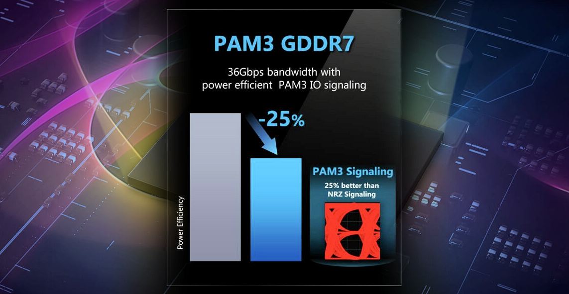
Samsung GDDR7 memory to offer 36 Gbps bandwidth, uses PAM3 signaling - VideoCardz.com
SAMSUNG confirms GDDR7 uses PAM3 signaling Coming to your PCs in the future. Samsung confirms that their next-generation GDDR7 memory technology will be up to 25% more power efficient than GDDR6 standard. The company reveals that this type of memory is using PAM3 (Pulse-Amplitude Modulation)...
 videocardz.com
"The GDDR7 memory technology is not expected to be used in graphics cards any time soon, furthermore, Samsung did not specify the timing and plans for the standard adoption yet...."Samsung GDDR7 memory to offer 36 Gbps bandwidth, uses PAM3 signaling - VideoCardz.com
SAMSUNG confirms GDDR7 uses PAM3 signaling Coming to your PCs in the future. Samsung confirms that their next-generation GDDR7 memory technology will be up to 25% more power efficient than GDDR6 standard. The company reveals that this type of memory is using PAM3 (Pulse-Amplitude Modulation)...
arandomguy
Veteran
RDNA4 is not going to be anytime soon either.
If there is no next generation memory with increased speeds next time (~2 years) around it's going to be interesting to see how that gets worked around.
If there is no next generation memory with increased speeds next time (~2 years) around it's going to be interesting to see how that gets worked around.
The expectation was a completely revamped shader core, not just a tacked on dual issue and some minor RT efficiency tweaks. What exactly are the significant changes?
What do you mean by "completely revamped"? If you mean totally new architecture, then you were just wrong. YOU WERE WRONG. Not AMD.
But dual-issue of FMA is anyway a significant change. It's not a thing that can be just "tackled" in. It does mean huge changes, even though it does not mean totally new architecture.
Also, the RT units got MUCH more improvements than just "minor efficiency tweaks", for example ray sorting and traversal is a BIG change.
So, you seem to be quite clueless about the actual technical changes AMD made with RDNA3 but you just rant because the wild speculation based on some misunderstood rumours ended up not being true and your expectations were way too optimistic.
Bondrewd
Veteran
It is completely revamped, they just never talked all the stuff they hacked out for PPAmaxxing purposes because AMD is silly.What do you mean by "completely revamped"?
Maybe at ISSCC.
At the same time, both AMD and Nvidia also seem to have more tools in the chest for improving effective bandwidth, so aren't quite as wholly reliant on memory chip speeds as before.RDNA4 is not going to be anytime soon either.
If there is no next generation memory with increased speeds next time (~2 years) around it's going to be interesting to see how that gets worked around.
But yea, the timing could maybe still work out for GDDR7 in late 2024. Not much to go on, though.
DegustatoR
Legend

AMD RDNA4 Rumored Specifications: Monstrous 129 FP32 TFLOPS GPU, GDDR7, 3.5 GHz Clock Rates And More
RedGamingTech has published a lot of information about the AMD RDNA4 architecture and upcoming Navi 41, Navi 42 and Navi 43 GPUs. This is one of the first leaks from a known leaker and while RGT has a reliable track record, this post is still being marked as a rumor at this point because...
AMD RDNA4 Rumored Specifications: Monstrous 129 FP32 TFLOPS GPU, GDDR7, 3.5 GHz Clock Rates And More
RedGamingTech has published a lot of information about the AMD RDNA4 architecture and upcoming Navi 41, Navi 42 and Navi 43 GPUs. This is one of the first leaks from a known leaker and while RGT has a reliable track record, this post is still being marked as a rumor at this point because...wccftech.com
Lol, only WCCFtech could get away with saying RGT “has a reliable track record”.
If you think about mathematics, if a ray hits a pixel on GDC 1 and is reflected to a pixel to GDC 2 this could lead to high bandwidth between GDC.I guess that's possible, e.g. by having some sub command processor per compute tile, with one main processor on the top. Not much new data flow besides the commands seems needed across the tiles then?
But initially i had assumed chiplets means the same revolution which happened to CPUs when going multi core, so we would see indeed multiple small GPUs.
Harder to saturate, but not impossible. I would still prefer it if it helps with pricing. I don't think this would be as disruptive as many people think. You still have only one VRam for all GPUs, and driver can help with translation of old games.
Though, it's still a revolution. AMDs market share is too small to establish this, and single device is their only option. Maybe this adds some thing to the respect they deserve for pioneering chiplets.
That's something that really found weird they didn't opt for a single big unified L3 as in their ryzen cpu line to avoid latency, specially on RT with several bounces required a big unifed L3 would avoid for better efficiency by avoiding wasting power from all the memory related ops and wasted bandwidth.
They just seem too focused on cost reduction but in the end performance seems to suffer and im not sure that trade off is worth it.
They just seem too focused on cost reduction but in the end performance seems to suffer and im not sure that trade off is worth it.
Bondrewd
Veteran
GPUs live and die on cost reductions per xtor.They just seem too focused on cost reduction
I think this an issue more related to L1 and L2 cache. I think there are the most values transfered.That's something that really found weird they didn't opt for a single big unified L3 as in their ryzen cpu line to avoid latency, specially on RT with several bounces required a big unifed L3 would avoid for better efficiency by avoiding wasting power from all the memory related ops and wasted bandwidth.
They just seem too focused on cost reduction but in the end performance seems to suffer and im not sure that trade off is worth it.
The GPU L3 is memory side cache, and is in a different clock domain from the shaders. (either fabric or memory clock)That's something that really found weird they didn't opt for a single big unified L3 as in their ryzen cpu line to avoid latency, specially on RT with several bounces required a big unifed L3 would avoid for better efficiency by avoiding wasting power from all the memory related ops and wasted bandwidth.
They just seem too focused on cost reduction but in the end performance seems to suffer and im not sure that trade off is worth it.
Whether it is “unified” or not has no significant bearing alone on the latency. If anything, the Ryzen CCX L3 Cache you mentioned is multi-banked (or “sliced” as they called it) similarly to provide higher bandwidth and parallelism. Just that it is architecturally private to the CCX, and clocked & placed so accordingly.
(edit: likely lower complexity and power usage as well, compared to a hypothetical “unified”, astronomically high associativity counterpart)
Last edited:
Similar threads
- Replies
- 318
- Views
- 23K
- Replies
- 85
- Views
- 18K
- Replies
- 85
- Views
- 12K
- Replies
- 185
- Views
- 20K
- Replies
- 59
- Views
- 8K