
nondescript
Regular
http://pc.watch.impress.co.jp/docs/2005/0722/kaigai199.htm
SCEI and PS3 development kit schedule announced
Sony Computer Entertainment held their yearly summary meeting for the Playstation, the PlayStation Meeting 2005. In that meeting, new information regarding the Playstation 3 was released.
First of all, the scheduled launch of the PS3 in the spring of 2006 was reconfirmed, and immediately before that, a pre-event called the “Playstation Conference†will be held.
At first, SCEI used the Cell Evaluation System to do software stack validation. This machine was supposedly used as a debugging machine, used in internal company labs, and it was also provided to a select group of vendors for evaluation. It has a 2.4 GHz Cell processor, 256MB XDR DRAM, and an nVidia graphics board.
Next, SCEI developed the much-anticipated “PS3 Evaluation System†for customer evaluation. The machine number is CEB-2030 and the codename is “Cytology.†SCEI has been distributing these machines to software vendors since this spring. The specs of the PS3 Evaluation System will be explained later, but basically it has a 2.4GHz Cell, 512MB of XDR DRAM, and a GeForce 7800 (G70).
In December 2005, SCEI is scheduled to release the “PS3 Reference Toolâ€, which has nearly the same architecture as the actual PS3. It will have a 3.2 GHz Cell, the RSX, 512MB of XDR DRAM, and a BD drive. Currently, it is set to be a 2U rack mount unit, but vertical configurations are being considered.
SCEI will continue to provide PS3 Evaluation Systems until November. Currently, 450 units have been sent out, and will continue to increase according to the supply figures shown below, to answer the intensive demand for the machine.
August – 200 units
Sept – 300 units
October – 3000 units
November – 3000+ units
CELL and XDR DRAM are 75% of PS3’s capability
The PS3 Evaulation System differs from the final PS3 specs in various ways.
First of all, the Cell operating frequency is 2.4 GHz, which is 75% of the production board. In the case of the CPU, it is not uncommon to hold down the clock speed until validation is completed. Of course, while it is not possible for this machine to perform at the PS3 final spec, the knowledge that it is at 75% [and then compensating for it] should be enough to get by.
The memory is XDR DRAM, and the Cell chip used is connected to the XDR DRAM by the XDR DRAM interface (XIO). This is also not full-spec. At least in June, the XDR DRAM date transfer rate in the PS3 Evaluation System was held to 2.4 Gbps. The PS3’s XDR DRAM data rate will be at 3.2 Gbps, so this is also a 75% capability.
The XDR DRAM data rate drop can be seen as in sync with the CPU clock speed drop. What this shows is the possibility that the Cell CPU core and the XDR DRAM interface were developed at the same time. Simultaneous development is easier, and has other advantages. Particularly, in the case of CPU-memory, latency is a very important factor, so simultaneous development has many advantages.
Most importantly, the XDR DRAM rate may have been dropped to compensate for the yield rate of the new XDR DRAM. It might be difficult to create 3.2 Gbps XDR DRAM samples at this early stage. If we think about the DRAM cell core clock (Internal Column Frequency), 3.2Gbps XDR DRAM is rather difficult. When XDR DRAM mass production for the PS3 begins, it will be moved to a 90nm process, but for now, it is being built on 100-110nm processes, which is bad for yield rates. Additionally, in the PS3 Evaluation System, RIMM (Rambus memory modules) are used. These modules might eat into the timing margins.
The PS3 Evaluation System introduced in this conference has a 512 MB of XDR DRAM. This is twice the 256 MB of the PS3. This increase might be due to the RIMM modules. In June, it was explained that the PS3 Evaluation System was designed to also be able to use RIMM. This large amount of memory is meant for verification [appraisal, testing] purposes.
The XDR DRAM interface is configurable, so it has high flexibility. It is an x16 interface, but is also capable being configured as x8 or x4. XDR DRAM has a point-to-point connection with the Cell chip. For example, by changing from x16 to x8, one channel can support connections with twice as many DRAM chips. The RIMM module takes advantage of this property, allowing one channel to support 2 RIMM while maintaining a point-to-point connection. (Trans. note: by context it is clear that “point-to-point†means a direct connection between two ICs, with no intervening chip in between.) On the other hand, the final PS3 design has the XDR DRAM memory directly integrated into the motherboard.
Currently, the graphics are connected by PCI-Express x4
In the PS3 Evaluation System, the PC-centric GeForce 7800 GTX (G70) is used as a substitute for the RSX. The RSX and G70 are made from about the same shaders, and the internal shader architecture is predicted to be quite similar. Because of that, as far as graphics are concerned, using the G70 as a base for software development should not create many problems. Shader programs should be able to run as if the two chips were the same.
However, the G70 has a lower clock speed than the RSX, and will certainly have some level of performance difference. However, an even greater difference than the internal GPU performance is the interface.
In the PS3, the Cell and RSX are connected by a parallel interface developed by Rambus called FlexIO (Redwood), which has a wide 35GB/sec bandwidth (20GB/sec down, 15GB/sec up). However, the G70, which has a PCI Express x16 interface, cannot be directly connected to the Cell’s FlexIO interface.
Therefore, in the PS3 Evaluation System the G70 is collected to the south bridge by PCI Express. In the June PS3 Evaluation System, they were connected by PCI Express x4. The south bridge used by the PS3 Evaluation System is basically the same as the south bridge developed by IBM for the Cell Workstation. Because of that, the chip has peripheral I/O PCI Express x4 meant for server applications. In the final version, PCI Express will disappear from the south bridge, but currently, the G70 is connected by it.
For that reason, currently the PCI Express x16 interface in the G70 cannot realize its full potential. According to the spec of the south bridge, Cell has only a 5 GB/sec FlexIO interface to the south bridge. If we assume the same is true for the PS3 Evaluation System, it will have drastically less bandwidth than the actual machine. Furthermore, the G70 is connected to the south bridge by PCI Express x4, which, at 2GB/sec, is even less. If we compare Cell->GPU bandwidth, we see that the PS3 Evaluation System is only 1/20 of the PS3.
According to SCEI, in the PS3 Evaluation System, the graphics side has been increased to 512MB of GDDR3 memory. In the actual PS3, there will be 256 MB of GDDR3. The reason for this increase in the video side memory is to allow buffering of data into the graphics side when the bus is idle. However, it will be difficult to use the PS3 Evaluation System to effectively evaluate the wide connection between the Cell and RSX in the PS3.
Additionally, the GDDR3 interface of the RSX is 128bits wide, whereas the G70 is 256bits wide, which means if both use x32 512Mbit DRAM chips, the G70 can support twice as much memory.
The special characteristic of the PS3 is the connection between Cell and RSX
The big special characteristic of PS3 Graphics is the connection between Cell and RSX. The RSX itself has a similar architecture to the G70, but the host interface for the G70 is meant for the PC and is completely different. The G70 uses PCI Express x16 to connect to the chipset as 8GB/sec (4GB/sec one-way), and it cannot directly access main memory. In contrast, the RSX has a 35GB/sec (20GB/sec down, 15GB/sec up) direct connection to the Cell, and can directly render from the main memory on the Cell side.
This is a big difference, because it allows a completely different way of using the GPU from PC architectures, SCEI explained. First of all, because the bus is wider, the Cell can perform a great amount of geometry operations, then send the vertex data [to the RSX]. Conversely, the RSX side can easily send data back to the Cell.
“The Cell processor can do both pre-processing and post-processing. For example, tessellation, dot filling, etc… Cell can perform physics processing like collision and motion calculations, and transform the vertex array.†said David B. Kirk, Chief Scientist of nVidia.
SCEI basically expects higher abstraction levels to be processed by Cell, and the details (like vertexes and pixels) to be processed by the GPU. The is reasonable – for example, in the case where the CPU side handles geometry transformation, collision detection, which is important in games, is not a problem. In the case where the GPU handles geometry transformation, if the data is not sent back to the CPU, clipping issues may occur. In the case of the PS3, the Cell side can perform transformations, and even if the GPU is used for transformation, it is comparatively easy to send the data back to the CPU side.
In architectures up to now, either the CPU or the GPU have been the bottleneck. It this is not resolved, we cannot go any further. To face this, in PS3 architecture, if the GPU becomes the bottleneck, it can shift work to the Cell, if the Cell becomes the bottleneck it can send work to the GPU, shifting the workload. For example, according to the software, the Cell side can perform more graphics processing, or, oppositely, or easily make an adjustment to leave the graphics work to the GPU, it was explained. In summary, between the CPU and GPU programmable processors, a flexible balance adjustment can be done.
In previous PC architectures, because they were limited by the CPU<->GPU pipe, geometry operations were held to a certain limit, and how rich an environment you can create within that limit became the main technical challenge. In contrast, the PlayStation2-type game consoles created large amounts of polygons, but after that it did not have the expressiveness of PCs. (Trans. note: probably means that PS2 is less capable in applying different effects to polygons than the PC, despite pumping out more polygons.) In the case of the PS3, both are possible, with the flexibility to balance the two.
However, in the case of the currently available PS3 Evaluation System, because of restrictions in the architecture, it is not possible to evaluate the balancing [of Cell and RSX]. This is a difficulty and a weakness, but, if we state it differently, software demos on the current systems still do not demonstrate the full potential of PS3. It is possible that the actual PS3 will have performance greater than current demos.
Significantly, when in comes to bus bandwidth, the Xbox 360 CPU-GPU connection is 21.6GB/sec, which is much wider than PCs. A wide-bandwidth CPU-GPU connections in not just the characteristic of PS3 in the next-generation consoles.
PS2’s simple boot-up started with firmware, and it loaded the OS and libraries from the disk. In comparison the PS3 starts from “Haipaabaiza†(Hyper-visor?) firmware. Haipaabaiza is a type of VMM (Virtual Machine Manager) software, which runs not on top but under the OS, providing machine virtualization. Even, when using only the Cell OS for gameplay, Haipaabaiza will always start first, and on top of that runs the pre-defined OS (guest OS). The OS, along with Haipaabaiza, creates a two-layer image. This basic OS layering is the same in the PS3 Evaluation System.
SCEI and PS3 development kit schedule announced
Sony Computer Entertainment held their yearly summary meeting for the Playstation, the PlayStation Meeting 2005. In that meeting, new information regarding the Playstation 3 was released.
First of all, the scheduled launch of the PS3 in the spring of 2006 was reconfirmed, and immediately before that, a pre-event called the “Playstation Conference†will be held.
At first, SCEI used the Cell Evaluation System to do software stack validation. This machine was supposedly used as a debugging machine, used in internal company labs, and it was also provided to a select group of vendors for evaluation. It has a 2.4 GHz Cell processor, 256MB XDR DRAM, and an nVidia graphics board.
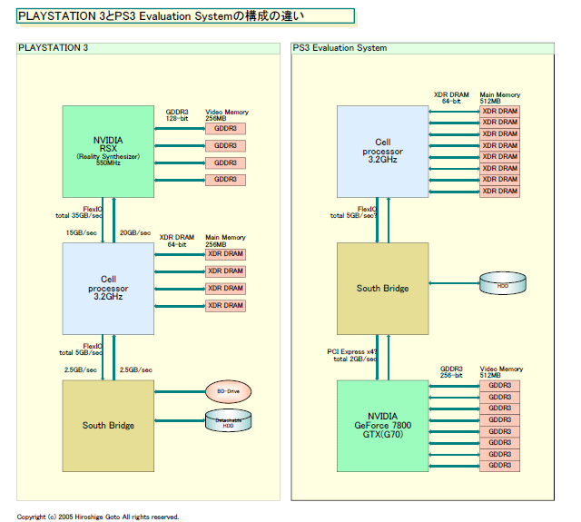
Next, SCEI developed the much-anticipated “PS3 Evaluation System†for customer evaluation. The machine number is CEB-2030 and the codename is “Cytology.†SCEI has been distributing these machines to software vendors since this spring. The specs of the PS3 Evaluation System will be explained later, but basically it has a 2.4GHz Cell, 512MB of XDR DRAM, and a GeForce 7800 (G70).
In December 2005, SCEI is scheduled to release the “PS3 Reference Toolâ€, which has nearly the same architecture as the actual PS3. It will have a 3.2 GHz Cell, the RSX, 512MB of XDR DRAM, and a BD drive. Currently, it is set to be a 2U rack mount unit, but vertical configurations are being considered.
SCEI will continue to provide PS3 Evaluation Systems until November. Currently, 450 units have been sent out, and will continue to increase according to the supply figures shown below, to answer the intensive demand for the machine.
August – 200 units
Sept – 300 units
October – 3000 units
November – 3000+ units
CELL and XDR DRAM are 75% of PS3’s capability
The PS3 Evaulation System differs from the final PS3 specs in various ways.
First of all, the Cell operating frequency is 2.4 GHz, which is 75% of the production board. In the case of the CPU, it is not uncommon to hold down the clock speed until validation is completed. Of course, while it is not possible for this machine to perform at the PS3 final spec, the knowledge that it is at 75% [and then compensating for it] should be enough to get by.
The memory is XDR DRAM, and the Cell chip used is connected to the XDR DRAM by the XDR DRAM interface (XIO). This is also not full-spec. At least in June, the XDR DRAM date transfer rate in the PS3 Evaluation System was held to 2.4 Gbps. The PS3’s XDR DRAM data rate will be at 3.2 Gbps, so this is also a 75% capability.
The XDR DRAM data rate drop can be seen as in sync with the CPU clock speed drop. What this shows is the possibility that the Cell CPU core and the XDR DRAM interface were developed at the same time. Simultaneous development is easier, and has other advantages. Particularly, in the case of CPU-memory, latency is a very important factor, so simultaneous development has many advantages.
Most importantly, the XDR DRAM rate may have been dropped to compensate for the yield rate of the new XDR DRAM. It might be difficult to create 3.2 Gbps XDR DRAM samples at this early stage. If we think about the DRAM cell core clock (Internal Column Frequency), 3.2Gbps XDR DRAM is rather difficult. When XDR DRAM mass production for the PS3 begins, it will be moved to a 90nm process, but for now, it is being built on 100-110nm processes, which is bad for yield rates. Additionally, in the PS3 Evaluation System, RIMM (Rambus memory modules) are used. These modules might eat into the timing margins.
The PS3 Evaluation System introduced in this conference has a 512 MB of XDR DRAM. This is twice the 256 MB of the PS3. This increase might be due to the RIMM modules. In June, it was explained that the PS3 Evaluation System was designed to also be able to use RIMM. This large amount of memory is meant for verification [appraisal, testing] purposes.
The XDR DRAM interface is configurable, so it has high flexibility. It is an x16 interface, but is also capable being configured as x8 or x4. XDR DRAM has a point-to-point connection with the Cell chip. For example, by changing from x16 to x8, one channel can support connections with twice as many DRAM chips. The RIMM module takes advantage of this property, allowing one channel to support 2 RIMM while maintaining a point-to-point connection. (Trans. note: by context it is clear that “point-to-point†means a direct connection between two ICs, with no intervening chip in between.) On the other hand, the final PS3 design has the XDR DRAM memory directly integrated into the motherboard.
Currently, the graphics are connected by PCI-Express x4
In the PS3 Evaluation System, the PC-centric GeForce 7800 GTX (G70) is used as a substitute for the RSX. The RSX and G70 are made from about the same shaders, and the internal shader architecture is predicted to be quite similar. Because of that, as far as graphics are concerned, using the G70 as a base for software development should not create many problems. Shader programs should be able to run as if the two chips were the same.
However, the G70 has a lower clock speed than the RSX, and will certainly have some level of performance difference. However, an even greater difference than the internal GPU performance is the interface.
In the PS3, the Cell and RSX are connected by a parallel interface developed by Rambus called FlexIO (Redwood), which has a wide 35GB/sec bandwidth (20GB/sec down, 15GB/sec up). However, the G70, which has a PCI Express x16 interface, cannot be directly connected to the Cell’s FlexIO interface.
Therefore, in the PS3 Evaluation System the G70 is collected to the south bridge by PCI Express. In the June PS3 Evaluation System, they were connected by PCI Express x4. The south bridge used by the PS3 Evaluation System is basically the same as the south bridge developed by IBM for the Cell Workstation. Because of that, the chip has peripheral I/O PCI Express x4 meant for server applications. In the final version, PCI Express will disappear from the south bridge, but currently, the G70 is connected by it.
For that reason, currently the PCI Express x16 interface in the G70 cannot realize its full potential. According to the spec of the south bridge, Cell has only a 5 GB/sec FlexIO interface to the south bridge. If we assume the same is true for the PS3 Evaluation System, it will have drastically less bandwidth than the actual machine. Furthermore, the G70 is connected to the south bridge by PCI Express x4, which, at 2GB/sec, is even less. If we compare Cell->GPU bandwidth, we see that the PS3 Evaluation System is only 1/20 of the PS3.
According to SCEI, in the PS3 Evaluation System, the graphics side has been increased to 512MB of GDDR3 memory. In the actual PS3, there will be 256 MB of GDDR3. The reason for this increase in the video side memory is to allow buffering of data into the graphics side when the bus is idle. However, it will be difficult to use the PS3 Evaluation System to effectively evaluate the wide connection between the Cell and RSX in the PS3.
Additionally, the GDDR3 interface of the RSX is 128bits wide, whereas the G70 is 256bits wide, which means if both use x32 512Mbit DRAM chips, the G70 can support twice as much memory.
The special characteristic of the PS3 is the connection between Cell and RSX
The big special characteristic of PS3 Graphics is the connection between Cell and RSX. The RSX itself has a similar architecture to the G70, but the host interface for the G70 is meant for the PC and is completely different. The G70 uses PCI Express x16 to connect to the chipset as 8GB/sec (4GB/sec one-way), and it cannot directly access main memory. In contrast, the RSX has a 35GB/sec (20GB/sec down, 15GB/sec up) direct connection to the Cell, and can directly render from the main memory on the Cell side.
This is a big difference, because it allows a completely different way of using the GPU from PC architectures, SCEI explained. First of all, because the bus is wider, the Cell can perform a great amount of geometry operations, then send the vertex data [to the RSX]. Conversely, the RSX side can easily send data back to the Cell.
“The Cell processor can do both pre-processing and post-processing. For example, tessellation, dot filling, etc… Cell can perform physics processing like collision and motion calculations, and transform the vertex array.†said David B. Kirk, Chief Scientist of nVidia.
SCEI basically expects higher abstraction levels to be processed by Cell, and the details (like vertexes and pixels) to be processed by the GPU. The is reasonable – for example, in the case where the CPU side handles geometry transformation, collision detection, which is important in games, is not a problem. In the case where the GPU handles geometry transformation, if the data is not sent back to the CPU, clipping issues may occur. In the case of the PS3, the Cell side can perform transformations, and even if the GPU is used for transformation, it is comparatively easy to send the data back to the CPU side.
In architectures up to now, either the CPU or the GPU have been the bottleneck. It this is not resolved, we cannot go any further. To face this, in PS3 architecture, if the GPU becomes the bottleneck, it can shift work to the Cell, if the Cell becomes the bottleneck it can send work to the GPU, shifting the workload. For example, according to the software, the Cell side can perform more graphics processing, or, oppositely, or easily make an adjustment to leave the graphics work to the GPU, it was explained. In summary, between the CPU and GPU programmable processors, a flexible balance adjustment can be done.
In previous PC architectures, because they were limited by the CPU<->GPU pipe, geometry operations were held to a certain limit, and how rich an environment you can create within that limit became the main technical challenge. In contrast, the PlayStation2-type game consoles created large amounts of polygons, but after that it did not have the expressiveness of PCs. (Trans. note: probably means that PS2 is less capable in applying different effects to polygons than the PC, despite pumping out more polygons.) In the case of the PS3, both are possible, with the flexibility to balance the two.
However, in the case of the currently available PS3 Evaluation System, because of restrictions in the architecture, it is not possible to evaluate the balancing [of Cell and RSX]. This is a difficulty and a weakness, but, if we state it differently, software demos on the current systems still do not demonstrate the full potential of PS3. It is possible that the actual PS3 will have performance greater than current demos.
Significantly, when in comes to bus bandwidth, the Xbox 360 CPU-GPU connection is 21.6GB/sec, which is much wider than PCs. A wide-bandwidth CPU-GPU connections in not just the characteristic of PS3 in the next-generation consoles.
PS2’s simple boot-up started with firmware, and it loaded the OS and libraries from the disk. In comparison the PS3 starts from “Haipaabaiza†(Hyper-visor?) firmware. Haipaabaiza is a type of VMM (Virtual Machine Manager) software, which runs not on top but under the OS, providing machine virtualization. Even, when using only the Cell OS for gameplay, Haipaabaiza will always start first, and on top of that runs the pre-defined OS (guest OS). The OS, along with Haipaabaiza, creates a two-layer image. This basic OS layering is the same in the PS3 Evaluation System.
")