Pascal FP16/FP32/INT8 Performance

Hey guys,

Wanted to start a clean thread on since it's a little hard to navigate the uber threads.

Just want to get a clean record for the various instruction rates of various Pascal based parts. NVIDIA has provided a sparse matrix of information. Of note is the restriction of FP16 on consumer parts and the special INT8 mode on Titan X. But how these specs fill in other GPUs isn't clear.

Would love to see this table (attached) filled out.

-James
 

Attachments

  • Screen Shot 2016-08-12 at 12.05.59 PM.png
    Screen Shot 2016-08-12 at 12.05.59 PM.png
    24.1 KB · Views: 101
GP100 is lacking dp4a and dp2a so that's a 0 in the int8 row.
Titan X (GP102) has only compatibility fp16, same as 1080 (GP104) so 1/64 (though it's really 1/128 vec2). It's also having only compatibility double support so 1/32 same as 1080.
The int8 is also full rate on 1080 so 4x of the fp32.
Also not that anything below fp32 is basically cuda only stuff.
 
That chart would be more useful if you added a DP4A row, which is the simple but useful new integer instruction in non-P100 Pascal.

Ryan did a great writeup of the fp16x2 compute in his GTX 1080 review. He shows a similar chart but also usefully extending back to Maxwell.

All Kepler, Maxwell, and Pascal GPUs have quad-rate Int8.
GP100 and Tegra X1 (Maxwell) have fp16x2, but no other NVidia GPUs do.
DP4A and DP2A (byte and word dot product accumulate) are on GP106, GP104, and GP102, but not GP100.
GP100 has 1/2 rate FP64, but GP106, GP104, and GP102 (TitanX) have 1/32 rate.
 
The vmad instruction in CUDA performs bytewise multiply-and-accumulate. Describing throughput rate ratios isn't as straightforward as fp32 since int32 mads are multiple instructions and not a single clock unlike fp32, hence giving vmad the throughput rate bonus relative to that baseline. And even more confusion comes with Kepler which has even higher throughput single clock 4-way SIMD byte operations (but not MAD). No NVIDIA GPU has 4-parallel-bytes-per-clock MAD, including the GTX 1080. I don't know if vmad is exposed to graphics compute.. it's not in CUDA C, but in CUDA PTX. Likely DP2A and DP4A will be exposed only in PTX as well but the final CUDA 8.0 documentation hasn't been released yet.
 
The vmad instruction in CUDA performs bytewise multiply-and-accumulate. Describing throughput rate ratios isn't as straightforward as fp32 since int32 mads are multiple instructions and not a single clock unlike fp32, hence giving vmad the throughput rate bonus relative to that baseline. And even more confusion comes with Kepler which has even higher throughput single clock 4-way SIMD byte operations (but not MAD). No NVIDIA GPU has 4-parallel-bytes-per-clock MAD, including the GTX 1080. I don't know if vmad is exposed to graphics compute.. it's not in CUDA C, but in CUDA PTX. Likely DP2A and DP4A will be exposed only in PTX as well but the final CUDA 8.0 documentation hasn't been released yet.
Int32 multiply seems to be roughly 1/3 rate on Kepler and Pascal (compared to fp32). Results here: https://devtalk.nvidia.com/default/topic/948014/forward-looking-gpu-integer-performance/

In comparison int32 multiply is 1/4 rate on AMD GCN. Int24 multiply is full rate on GCN (Nvidia no longer has fast int24 mul). It is very useful (as you rarely need full 32 bit muls), but unfortunately not exposed on PC DirectX. Bitwise ops and shifts are full rate on GCN. Nvidia has half rate shifts.
 
I will have a stupid question, its saturday night, so it shoulld be well on purpose.. is DP2A, DP4A are only Nvidia "instruction" term ( meaning it is impossible to compare witth anything outside Nvidia ? )..
 
Last edited:
Is there an exact description of DP2A/DP4A available somewhere? The names strongly hint at
dp2a= a0*b0 + a1*b1 + c
dp4a= a0*b0 + a1*b1 + a2*b2 + a3*b3 + c
but are these just (unsigned?) integer multiplications with (effectively) 32-bit integer additions?
 
Is there an exact description of DP2A/DP4A available somewhere? The names strongly hint at
dp2a= a0*b0 + a1*b1 + c
dp4a= a0*b0 + a1*b1 + a2*b2 + a3*b3 + c
but are these just (unsigned?) integer multiplications with (effectively) 32-bit integer additions?
Yes. Although I think there are signed variants. The real trick is the 32-bit accumulate.
 
Anyone have tested them in real code situations ? i have strange return from friends and at work ( who are coders, im not and thats a good reason for me to dont advance much in this aspect . )..
 
Last edited:
Nvidia: Eight bits ought to be enough for anybody ... doing AI
Roy Kim, a senior Nvidia product manager, told us the way forward is a "hybrid" approach, with a less-accurate model on the device so that decisions can be made immediately while a more powerful backend processes the situation and returns a more nuanced decision. State-of-the-art image-recognition systems have more than 150 layers of neurons, said Kim, hence the need for some more oomph on the inference side.

To maximize inference throughput, so your IoT personal-assistant-in-the-cloud doesn't leave you hanging for too long when you ask it a question, Nvidia has added two instructions to its Pascal architecture: IDP2A and IDP4A. These perform two and four-element 8-bit vector dot product calculations with a 32-bit accumulation.

The diagram of a single neuron below looks horrific but it's not as scary as you think. You've got values x1 to xn coming in on the left along n paths. Each xi input value is multiplied by its path's weight wi, and then the results of these multiplications are all added up. That's the dot product part.

Then that sum is fed into a threshold or activation function, and that output is fed into the next perceptron in the network.

perceptron.jpg

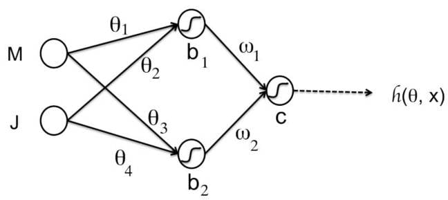
When you link these together you get something looking like this basic network, which has two inputs, three neurons, and an output.

nn2_example.jpg


So, ignoring the activation function, that top neuron's dot-product output is: (M x θ1) + (J x θ2). Now imagine those variables are each 8-bit integers ranging from -127 to 127, or 0 to 255. Now imagine doing up to 47 trillion of those dot-product operations a second, all combining inputs to feed into the next stages of a network. That's what Nvidia's P40 is claiming to do. That's what Nv means by accelerated 8-bit dot product calculations.

Nvidia also claims its P4 can do, at its very best, 21.8 trillion operations a second using 8-bit integers, and that the P4 is "40 times more efficient" than an Intel Xeon E5 CPU in terms of the number of images classified per second per watt using an AlexaNet-trained model.

The P4 and P40 will go on sale in October and November, we're told. If you really want to get your hands on similar kit now, Nv's Pascal-based Titan X graphics card, which emerged in July, can also do 44 TOPS of 8-bit integer operations. The P40 is basically a slightly beefier Titan X.

Meanwhile, Nvidia has released TensorRT, an inference engine to run on its hardware, and a software development kit called Deepstream, which can identify people and objects in high-resolution (HEVC, VP9) video.
http://www.theregister.co.uk/2016/09/13/nvidia_p4_p40_gpu_ai/
 
Seems like Nvidia is being really smart about how they segment their products:
– If you want high DP perf, must buy GP100
– GP100 is also the best card for training since it's the only desktop card that does 2x FP16. Assume FP16 is good for training but INT8 isn't.
– If you want really fast inference, must get P4/P40. Only "Tesla" variants have 4x INT8 perf. (not counting Titan X)
– If you buy a plain gaming card, eg GTX 1080, you don't get fast FP16, you don't get 4x IN8, and of course no usable DP64

- Yes and no, outside specific contract, GP 100 is not so easy to obtain . And it is not a " desktop " gpu.. ( only tesla server )

- Its a side effect, GP102 is a sku created after the initial Pascal, surely due to the cost and delay of HBM2, where they are really intellligent, is they add specific new "instructions" in between that was not initially on GP100 but can be used on a specific market, it was too add incentive to have this sku on the market ..
( sku who will certainly, after the TitanX,, been used too on the 1080TI )

The big problem of this generation, for both AMD and Nvidia is HBM2... both have delay their initial roadmap... Nvidia can release GP100 with HBM2 but, this sku is only available on selected contract for supercomputers, and others "Big company of AI, deeplearning" ( for automative ) ... AMD have delay the initial release ( Vega ) to 2017 ( or, as Nvidia, their initial roadmaps was point the 2016 gpu's ),

Well we could say, that Nvidia have somewhat keep track on their roadmap with GP100 for 3Dstacked memory ( HBM2 ), but honestly, it is not really "widly " available outside supercomputers center and other contracts ( who should been " up" and running " online on 2017-2018 if everything is going good anyway )
 
Last edited:
- Yes and no, outside specific contract, GP 100 is not so easy to obtain . And it is not a " desktop " gpu.. ( only tesla server )

- Its a side effect, GP102 is a sku created after the initial Pascal, surely due to the cost and delay of HBM2, where they are really intellligent, is they add specific new "instructions" in between that was not initially on GP100 but can be used on a specific market, it was too add incentive to have this sku on the market ..
( sku who will certainly, after the TitanX,, been used too on the 1080TI )

The big problem of this generation, for both AMD and Nvidia is HBM2... both have delay their initial roadmap... Nvidia can release GP100 with HBM2 but, this sku is only available on selected contract for supercomputers, and others "Big company of AI, deeplearning" ( for automative ) ... AMD have delay the initial release ( Vega ) to 2017 ( or, as Nvidia, their initial roadmaps was point the 2016 gpu's ),

Well we could say, that Nvidia have somewhat keep track on their roadmap with GP100 for 3Dstacked memory ( HBM2 ), but honestly, it is not really "widly " available outside supercomputers center and other contracts ( who should been " up" and running " online on 2017-2018 if everything is going good anyway )

You can buy the P100 here in the UK from at least one of the Nvidia service providors, not sure which one it was though and albeit within their own platform (does not need to be max configuration), but it is available now.
Cheers
 
You can buy the P100 here in the UK from at least one of the Nvidia service providors, not sure which one it was though and albeit within their own platform (does not need to be max configuration), but it is available now.
Cheers

You can order it ... and it willl b there when it can be ... I have not say it is not available .. But it can take time ..

But its not a problem, entreprise who order it have offtly nearly 1 year for put in places the process for upgrades, tests etcs ... We are not speaking about gamers upgrading ...

I can order one right now, and get one ,but if i want more and i have not a specific contract for it ... maybe ... in 1 year ..

Honestly, if it was so massively available, we will have return for the industry on the performance with the system who use it no? no tests, no leaks ---- no rumored perfomances, test numbers ..

But maybe you can provide me at least benchmark on how work the implementation of the HBM2 on Nvidia ? whats the performance of
it, does it bring somehing to the Pascall architecture ?


I will not imagine how everyone, as me, could compare, the GP 102 vs GP 100 when we think the GP100 is availlablle since nearly 6 months .....

Nvidia themselves was announces a GP100 in Q1 2017, in between they have release the GP 102 ...
 
Last edited:
Not as bad as it used to be it seems though.
By available I mean immediately (unless recently changed), but this is not all Nvidia service providors and in fact may only be 1 able to do this in the UK and I think it is part of their platform solutions that is certified, no idea for other regions.
I agree most will be doing orders for scheduled projects usually at least 3-6 months away for the initial phase, but then those tend to be larger scale deployments/research/academia.
Also key clients will be buying direct from Nvidia, but yeah this is made more complex as they also need to supply their partners such as Cray and IBM who could be ordering 1000s for each project.
But then the P100 is a rather special case GPU.

Cheers

Edit:
Also it seems prices are coming down for quoted single unit GPU, one of the solution providors is listing prices before discounts/etc as under $6k for the PCI-E 12GB, under $7.5K for PCIE-E 16GB, and under $10k for the mezzazine model. - caveat is these 'single' unit/non-platform (context not DGX-1 but a providors own certified solution platform) orders were not expected to be available until Sept/Oct.
 
Last edited:
Back
Top