NVIDIA Tegra Architecture

Discussion of Tegra's roadmap

In Nebu's post about the EDP driver he was very clear about the peak draw and how it was governed, and the fact the current SKUs were limited to less by the driver and the thermal budget.


His posts didn't need to concern themselves with perf/watt either. Stop picking holes in what he posted because you couldn't interpret it properly.

with the number of reactions, it seems that I'm not the only one to have interpretations problems... oh wait, maybe we just all understand perfectly :rolleyes:

anyway, discussion closed for me, back on technical stuff
 
with the number of reactions, it seems that I'm not the only one to have interpretations problems... oh wait, maybe we just all understand perfectly :rolleyes:

anyway, discussion closed for me, back on technical stuff
Maybe that's your own cognitive bias, because i didn't see a review, i saw a very explicit and exact detail that is 100% correct, if you look at other threads in this section he makes the same designation the same way on other SOC's.

Having a cry about negative bias of the person who uncovered there competitors cheating kind comes off a bit one eye'd dont you think?

Also having a hissy throwing the roll eyes and then saying im out is something my 5 year old does.....................
 
Perf/W is not at all what many have been trying to praise, this thing sucks a lot of power. Full load TDP is like 10W.


Rys - this is the quote that got me riled up. Notice it says Perf/W is bad, then talks about TDP (these are quite different things). Maybe Nebu does actually know what he's talking about, but the way the conversation started, I couldn't tell.
 
He doesn't really say it's bad. He says it's not what many have been trying to praise (different, but not casting a judgement), before leading into saying power is higher than people might expect. That affects things, especially at 10W.

So I think he's correct in saying perf/W isn't quite what it seems, using the facts that he brought to the thread to fuel more investigation.

There's so much nuance to this kind of analysis (and collectively as a discussion topic Beyond3D is new at it), so I understand that it's going to be difficult for all those commenting to get into the groove, form a common ground of terminology and understanding, and put all of the other building blocks in place to discuss it well.
 
The point was never that the user would see it. The point is that the SoC is capable of it, which is an interesting piece of factual data for everyone to understand.

Oh come on Rys. Any modern day GPU with modified BIOS and modified cooling can be overvolted and overclocked to the moon to consume much more power than normal. That part is very obvious, but it is pretty much irrelevant for the use cases for Tegra K1.

What Nebu did is take a debugging table for Jetson TK1, inexplicably correlated that with perf. per watt (even though he never actually measured performance nor power consumed at the voltage rails to achieve said performance), and then made a comment with negative connotation (and in support of an individual who has a history of trashing this company) about a peak consumption value that never gets seen in any real world device. And when presented with real world power consumption measurements of Jetson TK1, he ignored those and started calling several of us fanboys. So excuse us if some of us took that the wrong way.

That 10W is even a thing for fully embedded ARM-based SoCs is incredibly interesting.

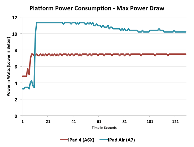
This was a "thing" months before Tegra K1 came to market. When running a mini power virus, the iPad Air can achieve ~ 11w for platform power consumption and ~ 8w delta between idle power consumption and load power consumption.

maxpower2sm.png
 
Last edited by a moderator:
Oh come on Rys. Any modern day GPU with modified BIOS and modified cooling can be overvolted and overclocked to the moon to consume much more power than normal. That part is very obvious, but it is pretty much irrelevant for the use cases for Tegra K1.
That was my point, that there's more than the tablet use case to consider for K1. T124 is also considered for automotive application, for example, where there's considerably higher potential power budget available.

What Nebu did is take a debugging table for Jetson TK1, inexplicably correlated that with perf. per watt (even though he never actually measured performance nor power consumed at the voltage rails to achieve said performance), and then made a comment with negative connotation (and in support of an individual who has a history of trashing this company) about a peak consumption value that never gets seen in any real world device. And when presented with real world power consumption measurements of Jetson TK1, he ignored those and started calling several of us fanboys. So excuse us if some of us took that the wrong way.
It's not a debugging table and it's not just for Jetson. The rest of your comment has been covered in recent posts. Again, the data he was providing didn't necessarily need to consider performance. It was just talking to power consumption.

This was a "thing" months before Tegra K1 came to market. When running a mini power virus, the iPad Air can achieve ~ 11w for platform power consumption and ~ 8w delta between idle power consumption and load power consumption.
I never said it was new, just that it was interesting to discuss in context.
 
Rys said:
Where's the discussion about what kind of products could be possible with K1 with active cooling if 20W was doable?

Drowned in a sea of bullshit because people feel obliged to defend the Shield Tablet and the K1 config therein. Enough; that's not what Beyond3D is about or for.
Speaking of bullshit... if that was Nebuchadnezzar's intention, I have a bridge for sell. Letting trolls troll, then defending them isn't what B3D is about either, or at least it shouldn't be...
 
He didn't troll this thread. He brought facts about the power management of the SoC and attempted to discuss them.
 
He didn't troll this thread. He brought facts about the power management of the SoC and attempted to discuss them.
He did bring facts to the table, but he also used some very weird and confusing terminology IMHO, and seemed confused on some things, e.g.:

Great for Nvidia if they have the dynamic range to be able to cap this to smaller values, but then what we're discussing nowdays is no longer hardware power consumption but to who has the best power management algorithms.
It's not just about the power management software, it's also about the hardware Perf/W at a given power envelope. Your power management algorithms might cap power and/or performance, but they won't magically improve Perf/W beyond what modern DVFS can do *at that cap*. It's still very much up to the hardware to be efficient enough overall. And hardware efficiency doesn't directly correlate to peak power either...
 
Rys said:
He brought facts about the power management of the SoC and attempted to discuss them.
In a distinctly negative light consisting generally of falsehoods. FUD.

Reading back through the series of posts, it is fairly clear he did not even have a proper understanding of what TDP means (or was being intentionally obtuse). Either way...

But don't take my word for it, browse through his post history....
 
Rys - this is the quote that got me riled up. Notice it says Perf/W is bad, then talks about TDP (these are quite different things). Maybe Nebu does actually know what he's talking about, but the way the conversation started, I couldn't tell.
Please do not blatantly misquote what I wrote, I wrote that it is not what it was hyped up to be and if you were following this thread over the last 8 months or so it was a notion in the ballpark of 2-3x the perf/W over competing products, which it clearly does not deliver no matter how much you misinterpret the data. My TDP post had nothing to do with the perf/W rant and I didn't mention both in relation to each other in any of my posts.

but they won't magically improve Perf/W beyond what modern DVFS can do *at that cap*. It's still very much up to the hardware to be efficient enough overall.
That is not true. Depending on *how* such a cap is implemented is what decides the perf/W, for example the granularity of the frequency limitation and if it it's allowing for higher DVFS points in burst versus a lower DVFS point over a more averaged period. The fact that the K1 has such a higher upper end in its dynamic range bodes badly for perf/W because the high frequency points are fed *extremely* high voltages for a 28nm HPm process. There are designers and programmers who do nothing but trying to optimize this relationship between DVFS latency, performance, and its resulting power consumption, it is very much a software problem and not only a hardware design issue.

Sure if you Overvolt and Overclock it.
No. This is on the stock frequencies, on the stock voltages, without any mysterious new BIOS or modifications. You and ams purely made this up in trying to rationalize your arguments.
Even better, it does it without any long term throttle as your test shows (more than 110 iterations of GFX bench before slightly going down).
With a magnesium heat shield the size of the tablet itself and with burning hot temperatures at the end of the test. Please.

-

I have nothing else to say that Rys didn't already bring up - he understood exactly what I wrote without having to get into any misinterpretations or arguments.
 
Last edited by a moderator:
I think it's fair to conclude that real-world tests paint the perf/W of the GPU in a good light, and not just at the higher ends of the curve.

But I'd still like to see some real measurements for CPU power consumption that go beyond running some web browsing loops. And I'm interested in what implications this alleged 10W CPU budget has. Does anyone know what frequencies deployed K1 hardware can sustain with all four cores active? I remember seeing some reports that Shield could run all four cores at 1.9GHz, then later hearing that it's ramped down to something like 1.4GHz.

In a presentation slide nVidia claimed roughly 1W per core at 2GHz and 1.6W at 2.3GHz. A 10W CPU budget implies that the CPU portion will be throttled to stay within no more than 10W, not merely that it can use up to 10W at maximum clock frequency with all cores active. This doesn't paint the CPU power consumption in nearly as good of a light as nVidia's slide has, even when taking into consideration the parts that are "CPU" that may be outside of the "cores."
 
In a presentation slide nVidia claimed roughly 1W per core at 2GHz and 1.6W at 2.3GHz.
I somewhat doubt those numbers; 2GHz is running at 1.22V and 2.3GHz at 1.36V nominal voltages before dynamic binning. That's insanely high for 28HPm. Qualcomm barely reaches or goes over 1V in the 801/805.
 
In a presentation slide nVidia claimed roughly 1W per core at 2GHz and 1.6W at 2.3GHz. A 10W CPU budget implies that the CPU portion will be throttled to stay within no more than 10W, not merely that it can use up to 10W at maximum clock frequency with all cores active. This doesn't paint the CPU power consumption in nearly as good of a light as nVidia's slide has, even when taking into consideration the parts that are "CPU" that may be outside of the "cores."
OTOH the cpu budget goes up to 10W in that table pretty quickly (for the high cpu load values) but doesn't increase at all from there, which could imply that this is usually sort of sufficient. If that's the case, that would still give 2.5W per core obviously, but 1.6W for some "average" instruction mix would sound fairly plausible then. Though my theory could certainly be wrong ;-).
 
Please do not blatantly misquote what I wrote, I wrote that it is not what it was hyped up to be and if you were following this thread over the last 8 months or so it was a notion in the ballpark of 2-3x the perf/W over competing products, which it clearly does not deliver no matter how much you misinterpret the data. My TDP post had nothing to do with the perf/W rant and I didn't mention both in relation to each other in any of my posts.
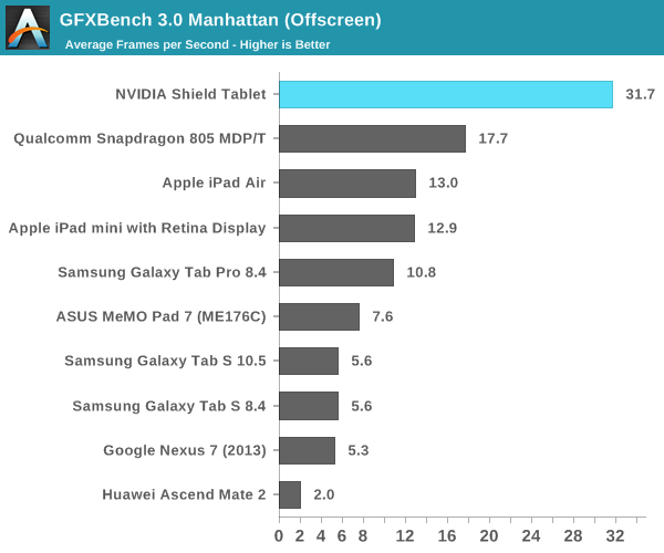
From you own website test, TK1 shows 2.5 times the A7 performance on Manhattan offscreen with very close power envelope, exactly where Nvidia predicted it...

65866.png


So contrary of what you say, it delivers. Stop the FUD.
 
From you own website test, TK1 shows 2.5 times the A7 performance on Manhattan offscreen with very close power envelope, exactly where Nvidia predicted it...

65866.png


So contrary of what you say, it delivers. Stop the FUD.

It shows much higher performance, yes, but I'm not sure where you get the power part.
 
From you own website test, TK1 shows 2.5 times the A7 performance on Manhattan offscreen with very close power envelope
How exactly is 6W vs 10W even *remotely* close in power envelope???

66% increased power for 2.5x the performance. Normalize them and you get a mere 50-60% better perf/W over the A7 while having a process node advantage.

Please stop wasting everybody's time.
 
With a magnesium heat shield the size of the tablet itself and with burning hot temperatures at the end of the test. Please.
Thanks for the magnesium shield, it doesn't throttle, unlike all snapdragon S8xx tablets currently in the market...
Xiaomi Mi Pad has no shield and it throttles... like others....
chose your poison... but for a gaming tablet, it makes sens.
again you try to put things only in the bad light, that's why people react to you. Try to be more objective and you will have different kind of responses...
 
Thanks for the magnesium shield, it doesn't throttle, unlike all snapdragon S8xx tablets currently in the market...
So you admit it has more to do with the thermal capacities of the tablet itself than the efficiency of the SoC? Thanks for agreeing with me.
Try to be more objective and you will have different kind of responses...
Pretty high claim to make while misrepresenting your power argument from just 2 posts ago.
 
Back
Top