NVIDIA Tegra Architecture

The easiest thing for NV would be to give further flexibility to the user via sw for less aggressive frequencies.

It is my understanding that NVIDIA has some flexible settings and different modes in Shield tablet to balance performance vs. power consumption. In the battery saver mode, the battery lifetime should be very competitive with other high end tablets. Hopefully we will find out soon.

As OlegSH alluded to earlier, I would much rather have a very playable 30-60fps for 3 hours of gaming rather than a very unplayable 15-25fps for 5 hours of gaming, but I would also appreciate having the ability to trade off performance for battery life when the extra performance isn't needed.

In the "max performance" mode, I would think that Tegra K1 application processor + mem. consumes ~ 4w with GFXBench 3.0 Manhattan Offscreen test (compared to ~ 2.5w for the A7 application processor + mem.).

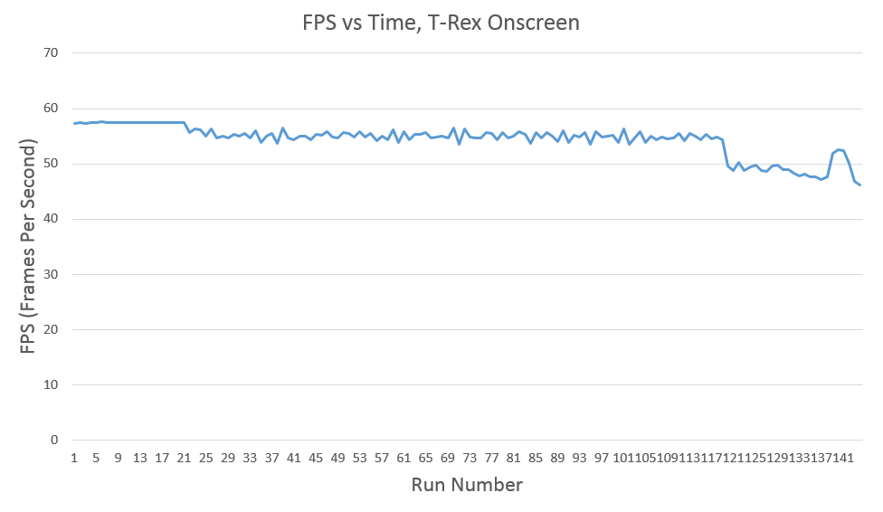
On a side note, I am very happy with the thermal dissipation capability of Shield tablet. Anandtech performed more than 115 runs of T-Rex HD Onscreen before there was any significant thermal throttling in Shield tablet.
 
Here are some tests for Xiaomi MiPad from http://www.ixbt.com/portopc/xiaomi-mipad.shtml
Epic Citadel Ultra High Quality
framerate
Xiaomi MiPad - 54,4 fps
Samsung Galaxy Tab S 8.4 - 46,4 fps
Samsung Galaxy Tab Pro 8.4 - 33,0 fps
LG G Pad 8.3 - 35,1 fps

Display brightness level is 100 nits for all devices
Battery lifetime for cycled Epic Citadel Guided Tour
Xiaomi MiPad with Max performance option - 5 hours 32 min. with 6700 mAh battery
Xiaomi MiPad with Battery Saving option - 7 hours 44 min.
Samsung Galaxy Tab S 8.4 - 2 hours 45 min. with 4900 mAh battery
Samsung Galaxy Tab Pro 8.4 - 5 hours 18 min. with 4800 mAh battery
LG G Pad 8.3 - 3 hours 28 min. with 4600 mAh battery

It seems K1 in Shield Tab has the discrete chip package compared to POP in Xiaomi, so Shield's K1 is less thermal constrained with less thermal throttling, therefore it's faster and more power hungry
 
Last edited by a moderator:
Do they have a score for K1 also in power saving mode? I wouldn't be surprised if its damn close to the original 54fps result. Citadel is beautiful to watch but as a GPU benchmark quite useless. Otherwise the K1 would get a LOT more than just 54fps.
 
Epic Citadel is a flawed benchmark. I don't trust its numbers. I mean the fps drops when lowering the resolution, there's definitely something funky going on with it.
 
Do they have a score for K1 also in power saving mode? I wouldn't be surprised if its damn close to the original 54fps result. Citadel is beautiful to watch but as a GPU benchmark quite useless. Otherwise the K1 would get a LOT more than just 54fps.
They don't have power saving score for this test for some reason, though the article's author noticed on forum that scores for Power Saving mode are 1/2 of Max perf mode for Manhattan HD onscreen/offscreen. "Guided Tour" is onscreen mode and should be vsync limited indeed, so framerate in power saving mode should be close to one in Max Perf mode
 
Half the Manhattan score sounds too aggressive for the power saving mode. Assuming they'd have an intermediate setting that might yield 2/3rd of the peak performance with say 3.5 hours battery life it could end up as a happy medium.
 
Perf/W is not at all what many have been trying to praise, this thing sucks a lot of power. Full load TDP is like 10W.

A few errors here.

First the power used is for the whole tablet (display, memory, network, etc) and not just the SOC.

Second the battery is rated as 5197 mAh, 3.8V chemistry (19.75 Whr) and since the tablet lasted 2.246 hours (full out gaming) means that the whole tablet was using 8.8 watts (19.75 / 2.246).

Third the tablet lasted 10.828 hours web browsing which works out to be 1.8 watts (19.75 / 10.828). Web browsing is pretty much a minimal impact on the CPU and negligible GPU power so I will use this number as the active base tablet power.

From this it appears that the SOC uses 7 watts full out gaming. 8.8 minus 1.8 equals 7.

And this number (7 watts) is a far far cry from the 20-30 watts a certain tech site published.
 
Obviously any claim of 20-30w power consumption is nonsensical and complete FUD at best, so nothing to be taken seriously.

On an aside, the Shield tablet actually has very competitive gaming perf. per watt. Keep in mind that in the T-Rex HD Onscreen test (used for battery lifetime estimate), Shield tablet is ~ 2.6x faster than the iPad Mini Retina, all while using higher quality rendering precision too. In a way it is almost comical to compare battery life with this particular test, because the iPad Mini Retina (and most other thin fanless tablets) does not even come close to having playable framerates while the Shield tablet handles it with ease.

One thing I don't quite agree with in the Anandtech review is the "battery performance" metric they used. It appears that they ran the T-Rex HD Onscreen test for more than 115 (!) runs before they were able to get any noticeable thermal throttling from the Shield tablet, and then they picked the lowest fps they could find after 141 (!) consecutive runs. In my opinion, the more realistic "battery performance" long-term data point is ~ 56fps in this test (and not the ~ 46fps that they showed in their comparison bar graph). In fact, even GFXBench lists the long-term data point as ~ 56fps (presumably what is recorded after ~ 30 loops of running this benchmark).

TRexRunDownGraph.PNG


I also noticed that Anandtech forgot to add the Surface Pro 3 data using the Core i3 processor (ie. the dual core processor used in the lowest cost $799 Surface Pro 3 variant). There is a significant difference in CPU/browser performance and 3dmark Unlimited performance when comparing Core i3 and Core i5 variants of Surface Pro 3. See "tablet" section in the middle of the page here: http://www.anandtech.com/show/8287/first-look-the-799-microsoft-surface-pro-3-with-core-i3
 
Last edited by a moderator:
A few errors here.
Absolutely no errors here. Nvidia themselves provide the numbers and they are inarguable.

The SoC at both CPU and GPU in full load has a 33W TDP which is artificially throttled down to either 17W or 12W depending on the model and divided between the CPUs or the GPU depending on CPU prioritization or GPU prioritization. This is all limited by thermals and what not, but that's the situation. The tablet SoC model has the 17W max "effective" TDP scenario because of the higher GPU frequency of 853MHz.

This is straight out of the electrical design power driver of the K1 which is in charge of managing the power budget of the chip.
Obviously any claim of 20-30w power consumption is nonsensical and complete FUD at best, so nothing to be taken seriously.
It's very real.
 
Last edited by a moderator:
The SoC at both CPU and GPU in full load has a 33W TDP
source ?
Official documentation of Jetson dev board gives completely different numbers and it was already verified true (by phoronix)

This is straight out of the electrical design power driver of the K1 which is in charge of managing the power budget of the chip.
It's not because the driver can output 33W that K1 consumes all of it... :rolleyes:
 
source ?
Official documentation of Jetson dev board gives completely different numbers and it was already verified true (by phoronix)
The official numbers don't matter in regards to what the chip is electrically designed for, the 10W or whatever figure is the throttling target.

kernel\arch\arm\mach-tegra\tegra12_edp.c

Code:
struct tegra_sysedp_corecap td575d_sysedp_corecap[td575d_sysedp_corecap_sz] = {

/*
TD575D/CD575M/SD575N
GPU MaxF	853000 KHz
CPU MaxBudget	10000  mW
*/
	/*mW	 CPU intensive load        GPU intensive load    */
	/*mW     budget  gpu(khz) mem(khz)  budget  gpu(khz) mem(khz) pthrot(mW) */
	{5000,  {1500,  108000, 933000}, {1500,  108000, 933000 }, 918 },
	{6000,  {3000,  108000, 933000}, {3000,  108000, 933000 }, 2109 },
	{7000,  {4000,  108000, 933000}, {3000,  180000, 933000 }, 2589 },
	{8000,  {5000,  108000, 933000}, {3000,  252000, 933000 }, 3068 },
	{9000,  {6000,  180000, 933000}, {2500,  396000, 933000 }, 3630 },
	{10000, {7000,  108000, 933000}, {3500,  396000, 933000 }, 4425 },
	{11000, {7000,  252000, 933000}, {4000,  468000, 933000 }, 5301 },
	{12000, {8000,  180000, 933000}, {3000,  540000, 933000 }, 5348 },
	{13000, {9000,  108000, 933000}, {5000,  540000, 933000 }, 6969 },
	{14000, {10000, 108000, 933000}, {3500,  612000, 933000 }, 6846 },
	{15000, {10000, 180000, 933000}, {4000,  648000, 933000 }, 7880 },
	{16000, {10000, 252000, 933000}, {3500,  684000, 933000 }, 8120 },
	{17000, {10000, 396000, 933000}, {4000,  708000, 933000 }, 9024 },
	{18000, {10000, 396000, 933000}, {3000,  756000, 933000 }, 9252 },
	{19000, {10000, 468000, 933000}, {4000,  756000, 933000 }, 10046 },
	{20000, {10000, 540000, 933000}, {5000,  756000, 933000 }, 10873 },
	{21000, {10000, 540000, 933000}, {3500,  804000, 933000 }, 10909 },
	{22000, {10000, 612000, 933000}, {4000,  804000, 933000 }, 11306 },
	{23000, {10000, 648000, 933000}, {4000,  853000, 933000 }, 12696 },
	{24000, {10000, 708000, 933000}, {5000,  853000, 933000 }, 13524 },
	{25000, {10000, 708000, 933000}, {5000,  853000, 933000 }, 13524 },
	{26000, {10000, 708000, 933000}, {6000,  853000, 933000 }, 14049 },
	{27000, {10000, 756000, 933000}, {7000,  853000, 933000 }, 15002 },
	{28000, {10000, 756000, 933000}, {8000,  853000, 933000 }, 15071 },
	{29000, {10000, 804000, 933000}, {8000,  853000, 933000 }, 15621 },
	{30000, {10000, 804000, 933000}, {8000,  853000, 933000 }, 15621 },
	{31000, {10000, 804000, 933000}, {8000,  853000, 933000 }, 15621 },
	{32000, {10000, 804000, 933000}, {9000,  853000, 933000 }, 16331 },
	{33000, {10000, 853000, 933000}, {10000, 853000, 933000 }, 17721 },
};

It's not because the driver can output 33W that K1 consumes all of it... :rolleyes:
Not because the driver can output? Sorry what?

The chip consumes up to 33W if it's totally let unrestricted, it's the driver which throttles it to one of the target TDPs by limiting the frequencies.
 
Don't be silly. The term "left unrestricted" is as nonsensical as can be. What that table above shows is that "MaxBudget" = 10w period (for Jetson TK1) at real world clock operating frequencies, and in any real world SoC this power budget needs to be allocated between CPU and GPU.

The only proper way to determine actual power consumed is to measure at the voltage rails using processor intensive applications. So with a GPU heavy load such as GFXBench 3.0 Manhattan, I would suspect that actual power consumed by GPU + mem. is ~ 4w in Shield tablet. Note that any TK1-powered tablet will also have a more power optimized platform compared to the Jetson TK1 dev kit.
 
Last edited by a moderator:
And speaking of Jetson TK1 power consumption, here are actual measurements and comments from a dev kit owner (https://devtalk.nvidia.com/default/...tk1-power-consumption/post/4218105/#4218105):

I have independently confirmed NVidia's power use estimates using a multimeter patched into the DC line. If anything, they are conservative. I never saw the board [ie. entire dev kit platform] exceed 12W under the most demanding use. I don't use SATA or some of the other ports, and some headroom might be required for that.

http://www.phoronix.com/forums/show...-Compared-To-AMD-AM1-APUs&p=416287#post416287

So unless you are really cooking the CUDA cores, the board is <8W and the chip <5W. When you decide to light a fire under all cores (CUDA smoke particle demo), the board is <12W and the chip <9W.

Hope that helps!
 
Don't be silly. The term "left unrestricted" is as nonsensical as can be. What that table above shows is that "MaxBudget" = 10w period (for Jetson TK1) at real world clock operating frequencies, and in any real world SoC this power budget needs to be allocated between CPU and GPU.

Well stated and good luck arguing with disciples of you-know-who. Actual hard data will be ignored as they don't fit the belief system.
 
Don't be silly. The term "left unrestricted" is as nonsensical as can be. What that table above shows is that "MaxBudget" = 10w period (for Jetson TK1) at real world clock operating frequencies, and in any real world SoC this power budget needs to be allocated between CPU and GPU.

The only proper way to determine actual power consumed is to measure at the voltage rails using processor intensive applications. So with a GPU heavy load such as GFXBench 3.0 Manhattan, I would suspect that actual power consumed by GPU + mem. is ~ 4w in Shield tablet. Note that any TK1-powered tablet will also have a more power optimized platform compared to the Jetson TK1 dev kit.
The max budget is a control value for the power modelling driver. It has all data and silicon characterisation constants that considers all physical interactions that would affect power consumption such as temperatures, leakage power, voltages and frequency. That 10W value is solely CPU related if you would read the code.

The fact that somebody measured a top 12W consumption is utterly uninteressting to the real TDP of the chip, the one that is not limited by the driver.
 
He measured < 12w for the entire Jetson TK1 platform. The application processor + mem. was always < 9w, and even that was with the most compute intensive CUDA smoke demo. In the real world, real measurements for both performance and power consumption matter, period.
 
In the real world, real measurements for both performance and power consumption matter, period.
They are absolutely meaningless to the discussions of the hardware when that power consumption can be simply altered by a one-line shell command in software.

I'm done arguing if fanboys aren't even willing to recognize Nvidia's own source code.
 
Nebuchadnezzar said:
The fact that somebody measured a top 12W consumption is utterly uninteressting to the real TDP of the chip, the one that is not limited by the driver.
I guess that means there are not "real" TDP measurements of any modern SoC. :rolleyes:
 
Look, this is a silly argument. No SoC is ever "left unrestricted" in any real world product.
Only recently have chip designers come up with more advanced power modelling or actual limiting mechanisms that consider power limitations between the various SoC elements. (Power budget, frequency limitation on either CPU or GPU side depending on load)

Most if not all SoCs before that did not care about such things and the only real limitation was a simple individual temperature throttling mechanism. You only have to go back 1 or 2 SoC generations to find these "left unrestricted" SoCs.

I guess that means there are not "real" TDP measurements of any modern SoC. :rolleyes:
And you'd be a fool to believe that they are. Qualcomm has been doing the same and Samsung and others recently too. "TDP" has become a meaningless characterization of a chip's power consumption because it will never represent what the hardware is capable of. Qualcomm openly admits this by saying that the S800 targeted 5-6W in tablets while 3.5W in phones.
 
Last edited by a moderator:
Back
Top