Install the app
How to install the app on iOS
Follow along with the video below to see how to install our site as a web app on your home screen.
Note: This feature may not be available in some browsers.
You are using an out of date browser. It may not display this or other websites correctly.
You should upgrade or use an alternative browser.
You should upgrade or use an alternative browser.
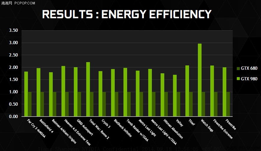
Close to 2x higher gaming perf. per watt for GTX 980 compared to GTX 680 without moving to an all new fab process node, pretty incredible!
Note that Maxwell--with it's significantly increased transistor count and it's superb energy efficiency--also appears to be a great fit for the much more transistor dense (but not much more energy efficient) 20nm fab process node at TSMC. This bodes well for their next gen Geforce, Quadro, Tesla, and Tegra [Erista] products due out within the next year.
It appears that we can expect to see GM210 (aka Big Maxwell) next year on a 20nm fab process node with close to 10 billion transistors (!) and with exceptional performance, energy efficiency, and transistor density.
Last edited by a moderator:
When was the last time that one company was truly ahead of the other in terms of architecture?
9800 (ATI), 8800GTX, RV770 and RV870, Maxwell ?
AMD better have an answer in the pipeline, otherwise winter is coming.
9800 (ATI), 8800GTX, RV770 and RV870, Maxwell ?
AMD better have an answer in the pipeline, otherwise winter is coming.
It appears that we can expect to see GM210 (aka Big Maxwell) next year on a 20nm fab process node with close to 10 billion transistors (!) and with exceptional performance, energy efficiency, and transistor density.
Unlikely, since Big Maxwell is already on it's way, first sightings were barely 2 months behind GM204
Look like Videocardz is definitively banned for get gpus themselves for reviews if they leak 2 reviews from other sites
They leak everything and then some, they don't do reviews themselves so they don't really have much to lose on that end
Unlikely, since Big Maxwell is already on it's way, first sightings were barely 2 months behind GM204
Unlikely regarding what exactly? This calendar year ends in only ~ 3 months. And Big Maxwell will need to make use of the much more transistor dense 20nm fab process node to dramatically improve upon Big Kepler (there is no room to grow die size and transistor count much beyond that of GK110 on a 28nm fab process node).
A1xLLcqAgt0qc2RyMz0y
Veteran
Unlikely regarding what exactly? This calendar year ends in only ~ 3 months. And Big Maxwell will need to make use of the much more transistor dense 20nm fab process node to dramatically improve upon Big Kepler (there is no room to grow die size and transistor count much beyond that of GK110 on a 28nm fab process node).
Wrong, they can/will grow die size.
Nvidia has been moving a sample of a GPU tagged as GM200 core (yes again). Earlier in July we noticed as well. This basically means that Nvidia has taped out the early A1 revision GPUs and engineering samples. This could mean a high-end launch Maxwell GPU as soon as Christmas IF wafer yields are decent enough.
...
This means that these processors will be HUGE in size, perhaps even over 620 mm²
http://www.guru3d.com/news-story/nvidia-gm200-(gtx-titan-ii)-spotted.html
It's probably a bit early to draw conclusions, but so far the energy efficiency is really what's amazing. So, compared to gk104, it's like a 33% increase in die size, with a 50% increase in transistor count, and the performance increase is somewhere along these lines. That is definitely ok (especially since it is done without a memory bandwidth increase) but not really extraordinary. However, that power draw apparently has gone down is quite an achievement - so "power/transistor" is only roughly half of what it was by the looks of it! Must have used a lot of low leakage, low power transistors, and I have no idea what other tricks (power gating, more fine grained clock gating...). And despite the low power design, it easily clocks higher too (of course it probably helps that there won't be any power delivery problems, but still...).
A1xLLcqAgt0qc2RyMz0y
Veteran
However, that power draw apparently has gone down is quite an achievement - so "power/transistor" is only roughly half of what it was by the looks of it! Must have used a lot of low leakage, low power transistors, and I have no idea what other tricks (power gating, more fine grained clock gating...).
Movement of data takes a lot of energy so optimizing data movement can save a lot of power.
See page 8 (Where is the Energy Going) of this PDF.
http://www.google.com/url?sa=t&rct=...OdMnbRzy2a6FV1A&bvm=bv.75774317,d.b2U&cad=rja
When was the last time that one company was truly ahead of the other in terms of architecture?
9800 (ATI), 8800GTX, RV770 and RV870, Maxwell ?
AMD better have an answer in the pipeline, otherwise winter is coming.
Any inherent advantage to Maxwell won't really be felt until the next process node. AMD still has a performance competitive part in Hawaii.
When was the last time that one company was truly ahead of the other in terms of architecture?
9800 (ATI), 8800GTX, RV770 and RV870, Maxwell ?
AMD better have an answer in the pipeline, otherwise winter is coming.
9700 for ATI then followed by the 9800 who was the logic suit... Anyway before speak about any advantage on architecture side, i will like to wait about AMD to release their architecture, because today its like comparing GK104-110 with maxwell when you want to compare it with AMD stuffs.
Last edited by a moderator:
Wrong, they can/will grow die size.
That's not really what Guru3D said. What they said is that IF there were problems with using a 20nm fab process (and I don't know why that would be the case given that high volume production has already started, although I can certainly understand not wanting to start on 20nm with a 10 billion transistor product), then GM200 (aka some Big Maxwell variant) would need to be manufactured on a 28nm fab process with what they speculated would be a "huge" die size.
Now that I think about it, GM204 already outperforms GK110 at only 398 mm^2 die size and only 165w TDP on 28nm fab process node, so it would be realistic to see a Maxwell variant on 28nm that is very close in die size and transistor count to GK110 that would still handily outperform GK110 at the same or even lower power envelope.
Last edited by a moderator:
Unknown Soldier
Veteran
Any reviews out yet? I thought the NDA ended 45 minutes ago?
That is true however Maxwell seems to look largely similar in overall structure so far to Kepler (at least on the hardware.fr diagrams...), I can't really see why the data would be a lot more local on average. But I guess improvements there are possible too even if you don't see them on the shiny block diagrams.Movement of data takes a lot of energy so optimizing data movement can save a lot of power.
Unlikely regarding what exactly? This calendar year ends in only ~ 3 months. And Big Maxwell will need to make use of the much more transistor dense 20nm fab process node to dramatically improve upon Big Kepler (there is no room to grow die size and transistor count much beyond that of GK110 on a 28nm fab process node).
Why exactly would Big Maxwell be smaller improvement over Big Kepler than GM204 is over GK104, respective to their die sizes?
Any reviews out yet? I thought the NDA ended 45 minutes ago?
Game 24 stream is going live now...
http://game24.nvidia.com/event
Megadrive1988
Veteran
Jen-Hsun is using GTX 680 / GK104 as a comparison with Maxwell and the target audience for upgrading.
Megadrive1988
Veteran
Yeah ^
Similar threads
- Replies
- 135
- Views
- 6K
- Replies
- 0
- Views
- 642
- Replies
- 123
- Views
- 23K