NVIDIA GF100 & Friends speculation

Sparse grid super sampling please :) These GPU's are so fast, that with the current gfx-progress= almost on hold, these forms of AA are easely usable.

I'am picking berry's in the woods of Cyrodill (heavely modded) with these modes and it looks just awesome (4xsgsaa) and I need two HD5970's in CF-X to maintain 60 fps :D
So with the faster Fermi two might be enough and I could get rid off the 4 way GPU scaling issues and have good fps with this mode.
But I'm so happy with the HD5xxx sgssaa IQ, that I demand at least on par IQ for Fermi, or the Radeons stay in my rig forver.
 
Last edited by a moderator:
Way more entertaining that way eh? ;)

Based on Nvidia's numbers Fermi's texture units are 60-100% more effective than GT200's. They claim a 70% gain in Crysis so assuming that's at a 1400Mhz clock that's 2x the throughput per unit per clock.

1.7 / (64*700)/(80*650) ~ 1.98x

If that's anywhere near the truth then things might not be as dire for Fermi variants as it seems on the surface.
Indeed. ;)

We'll see, you have to note though that your calcs are taking the absolute best case scenario (2x) and extrapolating from that, best case scenarios (& worst case) are after all corner cases.

I have no doubt that GF100 TUs will be more efficient, just how much I dont know. I wont take Nvidia's numbers for it either, until Rys has personally benched them. :D
 
I also ran a worst case scenario and it still wasn't that terrible. If we were to assume that Nvidia's numbers are from a higher clocked Fermi (1600Mhz) and a regular old GT200 running at 600Mhz, and use their L4D number (40%) we arrive at:

1.4 * (80*600) / (64*800) ~ 1.3x or 30% more efficient. I suspect the number will fall somewhere between 30 and 100% :p
 
my understanding, might be incorrect, is that the original mesh triangles are setup a 1 traingle per clock, but as tessellation takes place those triangles are 4 tris per clock.
 
Great example. With high tessellation, you drop from 500ish FPS in wireframe to just under 90. Without wireframe (i.e. shading, shadows and so in place), you go from 125ish to... 86ish. Talk about limitations.
Was AvP in NVidia's presentation?

Jawed
 
Of course. Setup just sees triangles, it doesn't know how they got there. There are 4 setup units, hence 4 per clock.

Jawed

That was my initial assumption but later comments re: tesselation threw that off.

Thanks for clearing that up. Thanks to Chalnoth as well.
 
I believe if they keep this design going forward from here, that if and when they put support for 3+ monitors on 1 card, they'd have a leg up on ATI unless they change the setup rate aswell. As the number of triangles being rendered across say 3 2" WS LCD is 3x as many as a single 24. Take Crysis, 5-6M triangles per scene, across 3 monitors you get 15-18M. For a good framrate of say an average 60FPS, your talking 900M to 1.04B triangles per seconded needed for that. So if GTX3xx can do 2400-2800M triangles/sec, had they done even just 3 monitors on one single GPU card, I'd say they'd have a very clear and distinct advantage.
 
I don't think the setup rate will in any way help to run more displays, as the primary limitation there is simply the fill rate. Basically, yes, you're drawing more triangles, but you're also drawing more pixels, so the pixel/triangle ratio doesn't change.

True, but the GTX3xx line will most likely be 40ROPs and 48ROPs, not sure how the 40ROP version would fair but the 48ROP version should fair decently with that kind of setup. GTX380 if and when it comes should have the fillrate to handle the trisetup rate, GTX360 maybe a bit different.
 
So only half that of Cypress (per clock)?
Strange they can think so different about the balance..
No Cypress is also "only" 32 pixels per clock (same as GT200).
For Fermi though it's now 32 pixels per half shader clock, instead of core clock, though so far it doesn't look like that'll make much difference, but it should be at least slightly higher.
Of course, mainstream parts will have both less rops and less GPCs, but how many is anyone's guess (though personally, I think just removing whole GPCs instead of disabling SMs withing GPCs should scale just fine).

Coulda swore Fermi was doing 40 and 48 pixels per half clock. GTX380 would have 6x8 ROP/PP and GTX360 5x8 ROP/PP(pixel pipes) that ran at half hot clock or are talking about something else in regards to that?
 
Thread open again, try and keep arch things in the arch thread if poss, and the rest in here. We're moving posts over to help this thread get everything it should have, but please do keep it all separate.
 
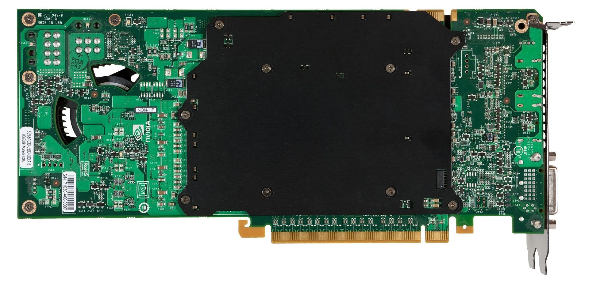
Some new pictures/slides of the Tesla variants.

NVIDIA CEO Showcases Fermi-based Tesla Graphics Card

Fermi_Tesla_02.jpg

Single 8 pin? (guessing that the other 6 pin connector isn't visible due to the angle of the pic)
 
Back
Top