NVIDIA GF100 & Friends speculation

pcinlife speculates that the upcoming GTX495 is cheaper than a HD5970, coming int at around €400.

http://translate.google.com/transla...le.pchome.net/content-1190503-30.html&act=url

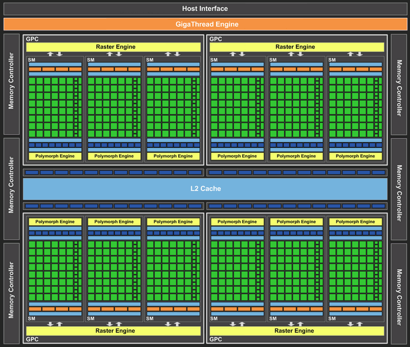
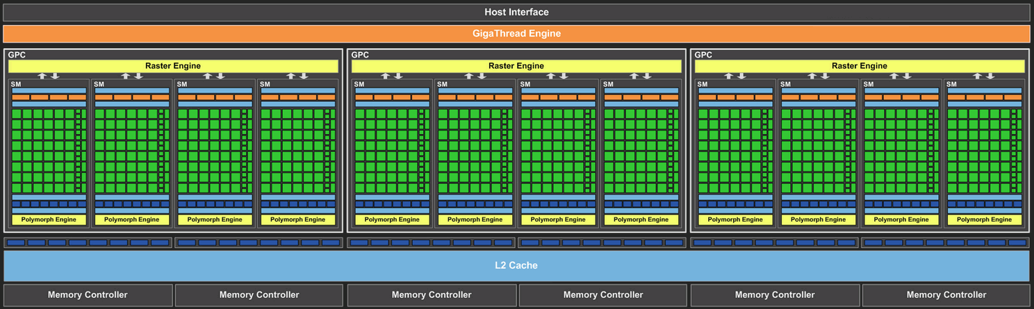
Bad Photshoppery is Bad
29w8vwl.jpg

400€ sounds like a great price. It also sounds reasonable, since I don't see the reason why it should cost more than two 460s in the first place. Maybe the chips are finer binned if they use full GF104, but we don't know that. Still, binning does not cost anything, right?

Anyway, regarding the "GTX 495" I was wondering of the following:

1) Will it have 1GB or 768MBs?
2) What is more probable, full GF104s or standard GF104s? I guess full GF104s would mean 2X1GBs.
3) Is it possible that Nvidia will implement some sort of Optimus technology in their GTX 495s, so they keep the card's idle power consumption to a bare minimum?

...and one more driver related really...

4) Is Nvidia's driver capable to let you use just one gpu in a quad sli setup? When you disable SLI what happens?

5) Would a GTX 460 1GB + GTX 495 Tri SLI setup would be possible, if the GTX 495 had 2X1gbs and "standard GF104s"?
 
There's some rumor floating, though, that nVidia has scrapped the dualchip plans and is going to introduce "GF110" asap, which would be GF104 but bigger.

Personally, though, I think the rumor above is just bullcrap, GF104 "made bigger" would face more or less the same problems GF100.
 
There's some rumor floating, though, that nVidia has scrapped the dualchip plans and is going to introduce "GF110" asap, which would be GF104 but bigger.

Personally, though, I think the rumor above is just bullcrap, GF104 "made bigger" would face more or less the same problems GF100.

While a dual-GF104 card would be pretty pointless against the HD 6000s in my opinion, I think a bigger GF104 (3GPCs?) would be more power-efficient than GF100. Probably still not enough against Cayman, though, and I'm afraid yields would be quite poor due to the die size.
 
There's some rumor floating, though, that nVidia has scrapped the dualchip plans and is going to introduce "GF110" asap, which would be GF104 but bigger.

Personally, though, I think the rumor above is just bullcrap, GF104 "made bigger" would face more or less the same problems GF100.
A 3 GPC GF104 would still be quite a bit smaller than GF100 and might beat (in a full config) GTX480 (with quite a bit lower power draw). Hence instead of the mythical rumored new stepping GF100 (haven't heard much from that lately) It could indeed make sense. Though in that case nvidia would have two huge chips with similar performance, one for workstation/compute, the other for desktop, which would be a bit odd. Also, I don't think GF100 problems only have to do with size, GF104 isn't really small neither yet still has much less problems (though we haven't seen that full config yet). I guess though to be competitive with Cayman they'd need a 4 GPC GF104, which would indeed be huge (550mm^2 again?).
Not sure though this rumor really can be true. Plans for dual chip cards can be scrapped (or made) in a relatively short time, but they would have to decide to build another chip quite some time ago.
 
Plans for dual chip cards can be scrapped (or made) in a relatively short time, but they would have to decide to build another chip quite some time ago.

Yup, would it be worth it to loose time and resources with something that is damned from the start?

Unless they would find a way to make a Dual GF100 with decent power draw :oops: That would be a big surprise.
 
Yup, would it be worth it to loose time and resources with something that is damned from the start?

Unless they would find a way to make a Dual GF100 with decent power draw :oops: That would be a big surprise.

You're seriously suggesting putting 2 chips, which of partly disabled one already consumes more than competitors dualcard with 29xW TDP, could be fitted on a dualchip card without breaking the 300W limit? Or even when ignoring the limit, get anywhere near decent powerdraw?
 
You're seriously suggesting putting 2 chips, which of partly disabled one already consumes more than competitors dualcard with 29xW TDP, could be fitted on a dualchip card without breaking the 300W limit? Or even when ignoring the limit, get anywhere near decent powerdraw?

Im not suggesting nothing. Re-read what I said. It would be a big surprise, and their "only way out", at the moment, IMO. It does not make sense, from the business point of view to make a Dual GF104, with new boards from AMD coming. But I dont think it will happen.
 
A 3 GPC GF104 would still be quite a bit smaller than GF100 and might beat (in a full config) GTX480 (with quite a bit lower power draw).
I'm not sure if 3 GPCs is physically feasible. Judging by how all other GF10x are shaped, I think you'd have to put them in a row, giving the chip an even odder shape than GF104 already has. And 35-40% more die area would already mean close to 500mm². Yields and power figures wouldn't be much better compared to GF100, I think.
 
I'm not sure if 3 GPCs is physically feasible. Judging by how all other GF10x are shaped, I think you'd have to put them in a row, giving the chip an even odder shape than GF104 already has. And 35-40% more die area would already mean close to 500mm². Yields and power figures wouldn't be much better compared to GF100, I think.
I don't think the SMs are that big, at least if I look at size of GF104 and GF106. Sounds more like 30% max larger to me - though granted it might be impossible to fit in some useful way (what about non-rectangular die, lol).
I don't agree that power consumption wouldn't be better, at least not if you compare against GTX480 - that thing draws twice as much max in practice as a GTX460 (forget about TDP on paper).
 
I don't agree that power consumption wouldn't be better, at least not if you compare against GTX480 - that thing draws twice as much max in practice as a GTX460 (forget about TDP on paper).

It honestly wouldn't vary too much.

Take TPU's 3dmark03 (1280x1024 4AA 16AF)numbers:
GTX480: 23424 =100%
GTX460: 13707 =58%
HD5850: 20862 =89%

Take TPU's Peak power draw (3DMark03 Nature at 1280x1024 6AA 16AF)
GTX480: 257W =100%
GTX460: 119W = 46%
HD5850: 108W = 42%

do you think the 460 design would stay more energy efficient or that the power usage would go up dramatically once it approached performance levels of the GTX480?

To demonstrate, I can just take the MSI's 460 Hawk numbers from the same test and compare it to the 470.
3dMark numbers:
GTX470: 18360 =100%
460Hawk: 15171 =82%
GTX460: 13707 =74%
HD5850: 20862 =113%

Peak power draw:
GTX470: 171W = 100%
460Hawk: 143W = 83%
GTX460: 119W = 69%
HD5850: 108W =63%

And the 460Hawk is even more energy efficient than other 460's as the numbers show (idle/BR tests) The average power draw shows a 1% delta from peak.
So I can't see how they can scale their current GF104 design up to GF100 levels but actually increasing their efficiency per Watt.
 
Last edited by a moderator:
I don't think the SMs are that big, at least if I look at size of GF104 and GF106. Sounds more like 30% max larger to me - though granted it might be impossible to fit in some useful way (what about non-rectangular die, lol).
I don't agree that power consumption wouldn't be better, at least not if you compare against GTX480 - that thing draws twice as much max in practice as a GTX460 (forget about TDP on paper).

Looking at the die-shot of GF100, I think the 4th quarter of area could be used for front end, ROPs and some blocks of memory controller...

Anyway, there is another way how to arrange 12 SMs, but 3 GPCs would take least die area.

 
If we take GF104 as a basis, a 768 ALU, 384 Bit GF100-successor should be entirely possible both within a power envelope of 300 Watts and a die size, that's, well, within spitting range of Nvidias biggest chip so far.
 
Why is that?

If the goal is the fastest chip with a given architecture inside both 300w power envelope and reticle limits at TSMC, i tend to disagree.

After all, Nvidia would want to be competitive with Cayman XT, wouldn't it?
 
Did you imagine how big would it be? GF104 has 367mm². Do you think nVidia is crazy enough to create a 600-660mm² GPU to compete with ATi's 380-400mm² GPU?
 
I don't know how their design cycle looked like this time, but I imagine some potential shrinks of individual units being quite possible.

How big is the portion of die space taken up by the ALUs & associated stuff? From a quick glance I'd say 60% or slightly less and I've read something that a GF104-style SM is about 25% bigger than in GF100 - that's what my assumption was based on.

Now, if we take this 60 percent of 530 mm², that's 318 mm², multiply with 1.25 and we get 397.5 mm². Add that to the remaining 40% and we'd be at ~610mm². Since larger chips generally have a slightly higher density and if I add my suspected optimization potential, I think it's possible to arrive at 580-590 mm².

Huge, but not impossible. The question is: Would Nvidia decide to take that risk?
 
Seems to be unlikely to me... even GF100 with one SM disabled can consume around 300W. It would be quite bizarre to see nVidia preparing an even bigger GPU to recover from problems caused by their previous big GPU(s)
 
Agreed, unlikely.
But on the power front they seem to have made progress, considering GF104.
And they might yet introduce a mechanism that is throttling the GPU if the power draw gets to high - just like AMD has wisely done in the 5000 series. That way, you might not have to take Furmark power draw by 2, but only „average gaming loads” or „commercially usable software”.
 
Back
Top