Hmm I wonder what they changed.Bios was not optimized ...
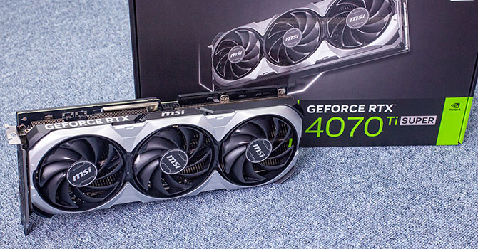
BIOS Update for Enhanced Performance MSI GeForce RTX 4070 Ti SUPER Series Graphics Cards
You are using an out of date browser. It may not display this or other websites correctly.
You should upgrade or use an alternative browser.
You should upgrade or use an alternative browser.
Nvidia GeForce RTX 40x0 rumors and speculation
- Thread starter Below2D
- Start date
DegustatoR
Legend
Making a wider bus is even more expensive than just putting twice the chips in a "clamshell" way. So all in all this shouldn't be a "preferred solution".Doesn't have to be as the 16GB 4060ti also shows, but the reality of Nvidia's product segmentation indicates that widening the bus was the only way you were going to get more than 12GB in this price class currently. The only other way would be to go clamshell and bump it up to 24gb, which was obviously never in the cards as that would throw the whole stack in disarray.
Thankfully G7 will kinda solve this finally by providing 1.5x memory chip density steps.
Hmm I wonder what they changed.
It's actually a good question. I'm actually not certain what is contained in a videocard bios that would affect performance. I would guess all of the voltage to frequency curve stored in bios? Should have I would guess all of the VRAM timings, frequency, voltage etc are. Is there other firmware on a gpu, or is most stuff contained within the driver? All of the software to drive the front-end should be in the driver, no? BIOS would have more general stuff like identifiers and interfaces for the drivers, no?
Some speculation was that it was power related but tests I saw showed it running 285W like normal. Not sure about clockspeeds but IIRC they weren't out of spec.It's actually a good question. I'm actually not certain what is contained in a videocard bios that would affect performance. I would guess all of the voltage to frequency curve stored in bios? Should have I would guess all of the VRAM timings, frequency, voltage etc are. Is there other firmware on a gpu, or is most stuff contained within the driver? All of the software to drive the front-end should be in the driver, no? BIOS would have more general stuff like identifiers and interfaces for the drivers, no?
DavidGraham
Veteran
Several years ago, we had a similar situation with the RX 5600XT, but it was quite different, as the release BIOS for the card had lower memory clocks (12Gbps) which was lower than what AMD specified, AMD then rectified the situation with a new BIOS to up the clocks to 14Gbps.It's actually a good question. I'm actually not certain what is contained in a videocard bios that would affect performance.
This time, it seems the MSI 4070TiS boards were experiencing a power problem that reduced the GPU boost clocks, according to TPU.
Interestingly, between BIOS updates, MSI never changes the rated boost clock (always 2610 MHz), the power limit wasn't increased either (always 285 W)
"Still the GPU frequency increased. I did some quick testing and it seems that something else on the PCB was drawing excess power, which left less power for the GPU, which meant it ran into the power limit earlier and couldn't boost higher.

MSI GeForce RTX 4070 Ti Super Ventus 3X Review
The MSI GeForce RTX 4070 Ti Super Ventus 3X comes a triple-slot, triple-fan cooler that achieves excellent noise levels. Unfortunately the card required two BIOS updates to bring it closer to expected performance, and the story might not be over yet.
D
Deleted member 2197
Guest

Nvidia just swapped the GPU in some of its RTX 4070 graphics cards
Normally made using a small AD104 GPU, new variants of the RTX 4070 have been spotted that use the much bigger AD103 used in the RTX 4080.
Nvidia is apparently allowing graphics card manufacturers to make GeForce RTX 4070 cards out of GPUs normally used in its much more powerful graphics cards. Specifically, instead of using the AD104 chips used in standard cards, an Nvidia GeForce RTX 4070 made with the AD103 GPU normally found in the RTX 4080 has been discovered.
...
The discovery was made by TechPowerUp, thanks to a reader submitting a screenshot, which showed GPU-Z failing to recognize this particular card. GPU-Z is TechPowerUp’s widely used graphics card information software, and after analyzing the submission data from the app, the site discovered it was being flagged as using an AD103 chip, rather than the expected AD104.
davis.anthony
Veteran
I would love for this to be another GTX 465 scenario 
Last edited:
DegustatoR
Legend
Will be the exact same spec with zero practical difference. Could maybe overclock a bit better due to die size differences?I would love for this to be another GTX 265 scenario
The only differences that could really be are related to which units are disabled and which enabled and whatever possible latency penalties (probably nothing measurable in practice) it might result in if enabled/disabled units are stacked together vs spread out (which then could bring miniscule thermal benefits)Will be the exact same spec with zero practical difference. Could maybe overclock a bit better due to die size differences?
As for OCing, more likely it should be worse rather than better if there's a difference, since bigger chips in general clock slightly worse simply for being bigger
DegustatoR
Legend
Chips are the same, die area is different though and if the clocks were limited by power/temps on a smaller one they could go higher on these. Still the difference is unlikely to be practically noticeable.As for OCing, more likely it should be worse rather than better if there's a difference, since bigger chips in general clock slightly worse simply for being bigger
I meant the pure physics side of it, bigger die means longer tracesChips are the same, die area is different though and if the clocks were limited by power/temps on a smaller one they could go higher on these. Still the difference is unlikely to be practically noticeable.
DuckThor Evil
Legend
What was that? Perhaps you mean the GTX 560 Ti 448 core edition?I would love for this to be another GTX 265 scenario
davis.anthony
Veteran
There was a typo, I meant GTX 465.
For those that wasn't around back then, the GTX 465 used the larger die of the GTX 470 and not the die the GTX 460 used.
And it turned out that a lot of the GTX 465's were quite literally GTX 470's, and they even had the extra RAM chips on the PCB (GTX 465 spec was 1GB VRAM where as GTX 470 was 1.2GB VRAM)
It was completely soft locked via the BIOS and flashing a reference GTX 470 BIOS on to a GTX 465 unlocked the full GTX 470 spec, including enabling the extra VRAM.
It's won't happen with the 4070 but it's nice to dream
Higher leakage as well, plus cut down dies are typically lower bins.I meant the pure physics side of it, bigger die means longer traces
You could do the same back with the X1800GTO even further back in the day (circa 2006 I think?) I bought one hoping to flash it to a X1800XT but unfortunately mine didn't unlockThere was a typo, I meant GTX 465.
For those that wasn't around back then, the GTX 465 used the larger die of the GTX 470 and not the die the GTX 460 used.
And it turned out that a lot of the GTX 465's were quite literally GTX 470's, and they even had the extra RAM chips on the PCB (GTX 465 spec was 1GB VRAM where as GTX 470 was 1.2GB VRAM)
It was completely soft locked via the BIOS and flashing a reference GTX 470 BIOS on to a GTX 465 unlocked the full GTX 470 spec, including enabling the extra VRAM.
It's won't happen with the 4070 but it's nice to dream
It used to be almost the norm. Everyone wanted 9500 Pro "L-version" because it could be flashed to 9700 (Pro) for example.Higher leakage as well, plus cut down dies are typically lower bins.
You could do the same back with the X1800GTO even further back in the day (circa 2006 I think?) I bought one hoping to flash it to a X1800XT but unfortunately mine didn't unlock
davis.anthony
Veteran
You could do the same back with the X1800GTO even further back in the day (circa 2006 I think?) I bought one hoping to flash it to a X1800XT but unfortunately mine didn't unlock
Yes there has been a number of GPU's you could flash to the higher spec SKU's.
The last GPU's that I believe you could BIOS flash was the AMD R9 200 series where you could flash the R9 290 to an R9 290x.
arandomguy
Veteran
Early r9 fury cards could be flashed to r9 fury x as the hardware was disabled via bios, later ones were disabled via fuse or laser (not sure which).
Early rx 480 4gb cards had 8gb memory physically but disabled via the bios, they could be flashed to 8gb.
Early rx 480 4gb cards had 8gb memory physically but disabled via the bios, they could be flashed to 8gb.
davis.anthony
Veteran
Early r9 fury cards could be flashed to r9 fury x as the hardware was disabled via bios, later ones were disabled via fuse or laser (not sure which).
Early rx 480 4gb cards had 8gb memory physically but disabled via the bios, they could be flashed to 8gb.
I took a break from PC gaming after the R9 290 series so I wouldn't have known there were cards released after that could still be unlocked vis BIOS flash.
DegustatoR
Legend

NVIDIA GeForce RTX 4070 GDDR6 Launches Today: Same GPU Specs, Same Price, Same Performance, Tweaked G6 Memory To Meet Huge Demand From Gamers
NVIDIA's GeForce RTX 4070 GDDR6 GPU launches today, offering same performance, same specs and same prices as the GDDR6X models.
Similar threads
- Replies
- 11
- Views
- 2K
- Replies
- 590
- Views
- 76K
D
- Replies
- 7
- Views
- 3K
