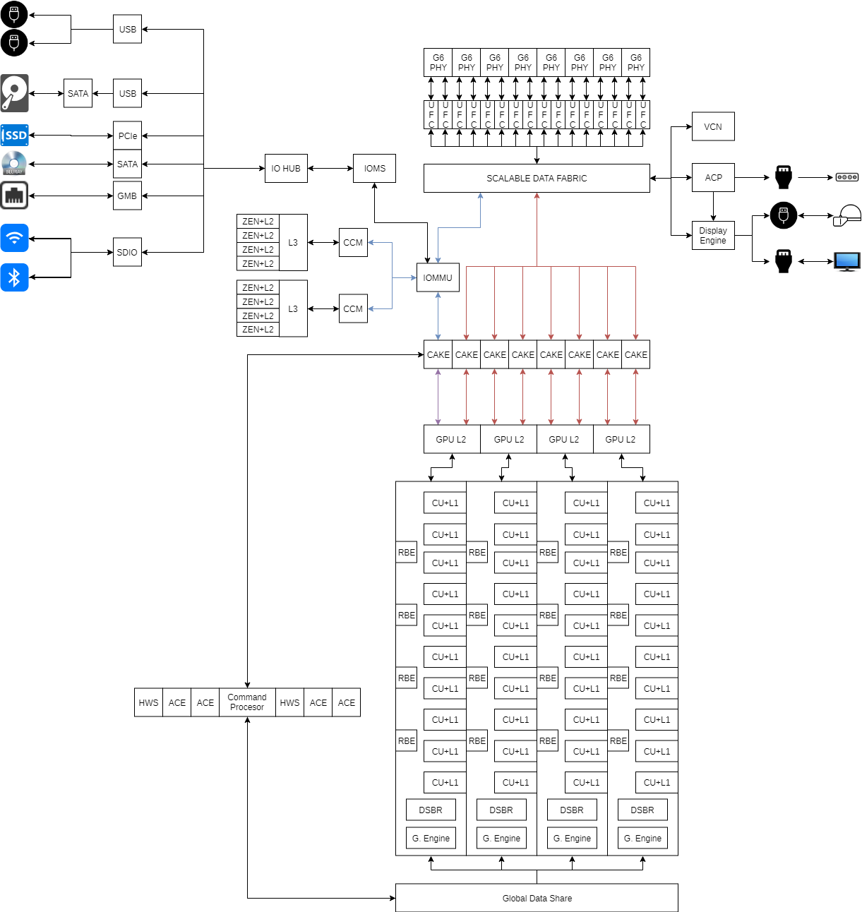
I'm unclear on whether this is split across multiple chips, or if it's one die. The CAKE is used to translate packets on the SDF into a form to be passed over the SERDES of an off-chip link, and on the other chip a SERDES and then another CAKE would convert the packet into the form used by the SDF.
At least from data given for EPYC, the path is SDF->CAKE-> serial link (IFOP, IFIS, etc.) ->CAKE->SDF. Units like the GPU wouldn't plug directly into a CAKE, and if this is one chip the CAKE wouldn't be necessary.
(
https://www.slideshare.net/AMD/amd-epyc-microprocessor-architecture slide 17).
A CAKE is a Coherent AMD Socket Extender (
https://www.slideshare.net/AMD/isscc-2018-zeppelin-an-soc-for-multichip-architectures, slide 8), and at least in part the way the GPU front end still works as is a PCIe slave device over a non-coherent connection. For an APU like Raven Ridge, the GPU supposedly has two interfaces onto the SDF, however what type of interface they are isn't clear. GPUs tend to be treated as IO devices with the IOMMU, which may mean that a GPU plugged into the SDF is likely using an IOMS rather than CCM.
For Zen, CCM is what serves as a CCX's port onto the SDF, and at least from that there's no need for the IO Memory Management Unit to intercede. The cores have their own MMUs and TLBs as hosts, whereas slave processors are kept behind the IOMMU. Most likely, going from the diagrams already given and from AMD's PPR document (
https://www.amd.com/system/files/TechDocs/54945_PPR_Family_17h_Models_00h-0Fh.pdf pg 28), the IOMMU is part of the IO complex, and is part of or linked to the IOMS. The IOMS would serve as the point of entry of IO into the SDF, with the CPUs not linking to it.
As ancillary controllers/IO, I'm not sure the ACP or display engine would link directly into the SDF rather than the IO Hub or some kind of IOMS.
As for the GPU L2s, it might be plausible at the TFLOP levels in question that more than four slices would be present.
The relationship between the command processor and ACE blocks and the L2/memory isn't entirely spelled out for GCN, although they should have the ability to use the L2. I'm not sure what other paths they have, though a CAKE is unlikely to be something they'd link to directly.
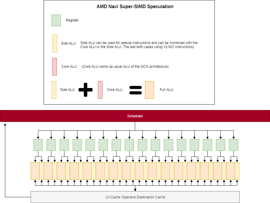
The patent has an embodiment where the ALU block is more like one Core ALU that can pair with a Side ALU, and another Core ALU. The patent doesn't limit itself to any one specific combination, although in that embodiment a Core ALU has a multiplier that makes it more suited for the primary set of instructions, while the Side ALU only has an adder and ancillary hardware for assisting a Core ALU on an complex op. A Core+Side is needed to get the full range of operations of a traditional GCN unit.
As far as the diagram goes, the two Core ALUs have straight links to the operand network, while the Side ALU hangs off their ports. The destination cache also feeds into the register file or operand network, rather than the scheduler. As far as an L0 cache goes, the related patent on the register file has the output flops of the register file labelled as an L0.
Part of the motivation for the destination cache is that it can feed back into the ALU operand ports, since the register file itself has lower peak bandwidth than the ALU blocks require.


