Next Generation Hardware Speculation with a Technical Spin [pre E3 2019]

Status
Not open for further replies.
AMD could save on the costs of interposer if they used Intel's EMIB (Embedded Multi-Die Interconnect Bridge) approach.

This would need a bigger package though, as all IO contacts must be very closely aligned - resulting in an elongated die on the sides where EMIB connections are engaged.

It's also an Intel exclusive so far, with no roadmaps from AMD or other chip makers.

Vita had stacking [but with side bridges, no vertical bandwidth paths to two 256MB RAM chips and one 128MB VRAM chip]
New+Picture+%25281%2529.png

New+Picture+%25282%2529.png
 
That's talked about generally in The Console Hardware thread. The decoding maps to a lot of unknowns. So far without anything definitive. Dont waste any more time on it.
 
More Navi rumors
To me, most notable thing from this is that Navi will be spiritual successor of Polaris [which was price/performance king of its time], that it will skip the biggest mistake of Polaris [who had it high performance part canceled due to belief that Vega+HBM could replace it], and that it will be focused on GDDR6.

All that sounds good.

If this summer Navi 10 is close to 2070 for much cheaper price, I will be glad.
 
That was fantastically unhelpful. There's some sort of guide, that then doesn't seem to correspond at all to what I'm looking at? I don't know how you got 1.8ghz out of that thing, what am I missing? : (

Unhelpful ? In what sense ? He (Apisak) said he is just guessing the gpu clock.... thats why there is question mark.
The point was that the code name "Navi Lite" is connected with conzole and that APU will use 8 zen cores
 
In that case, would there be any benefit to including a heatsink on the underside of a PCB without passing through it too? So it needn't interfere with the HBM data paths, but could still cool the lower layers?
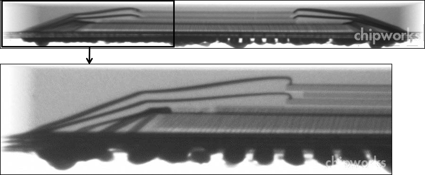
That places many layers of material between the active silicon and the heatsink. I am not sure if you meant PCB as in the motherboard, that's several layers of insulation, then the layer of solder balls for the chip package, then multiple layers of the package, then the interposer, then the base area of the stack.
There is some heat transfer capacity for a chip through its traces into the motherboard, for a limited amount of dissipation. That tends to track with limited power consumption and a sufficient ratio of connected traces in the PCB.
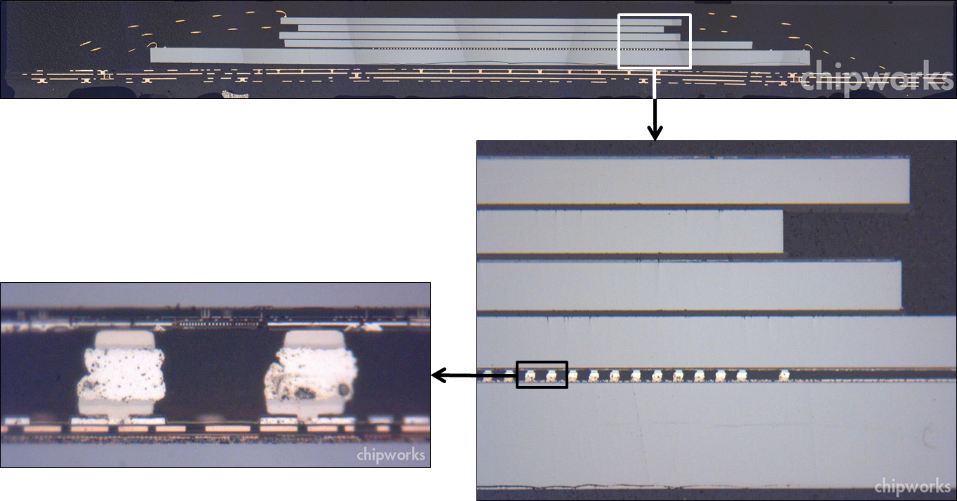
HBM's distance from the board is greater, and more of its smaller connections provide don't go very far since they're in the interposer and go straight to the SOC.

If you meant getting the heatsink up to the base of the chip package or up to the base of the interposer, it might be closer. Wires need to be routed around it, pad area between each layer needs to be sacrificed, and the mechanical properties shift. The amount of transport and how well it would turn out in models or implementation is outside of my sphere of expertise.

Or maybe feed a thermally conductive top layer with both the main, top heatsink, and cascade thermally conductive wires down the sides of the HBM stack to the bottom heatsink too?
The small cross section of the wires and distance traveled seem like they would limit the dissipation through the wires. The underside heatsink patent put much more metal through the PCB and package to the chip in order to provide a lower thermal resistance path.
 
8 cores is disappointing considering that many of them are going to be wasted for the os as usual.

I was hoping for 12 cores of which 8-9 available to games
 
8 cores is disappointing considering that many of them are going to be wasted for the os as usual.

I was hoping for 12 cores of which 8-9 available to games


Well, given how zen+ cores are much more capable than jaguar core in todays console, I still think it's a big, big boost, very needed, even of "only" 7 cores are really available, maybe with smt in top of that.

And I don't want to pay my PS5 699€ because of 2 more cores :eek:
 
Status
Not open for further replies.
Back
Top