Install the app
How to install the app on iOS
Follow along with the video below to see how to install our site as a web app on your home screen.
Note: This feature may not be available in some browsers.
You are using an out of date browser. It may not display this or other websites correctly.
You should upgrade or use an alternative browser.
You should upgrade or use an alternative browser.
Next Generation Hardware Speculation with a Technical Spin [2018]
- Thread starter Tkumpathenurple
- Start date
-
- Tags
- 5 bytes
- Status
- Not open for further replies.
So the cat's out of the bag: there's already a console out there using Zen cores. It should be pretty safe to assume the Jaguar architecture isn't coming back.
Much higher clock speed as well, next-gen is going to be a huge jump in CPU power. Also, it doesn't seem that big:

And that's at 14nm, at 7nm we should hopefully get something much faster in next gen consoles. Zen 2 + 8C/16T + 16GB GDDR6 as a base seems a good place to start with imo.
Much higher clock speed as well, next-gen is going to be a huge jump in CPU power. Also, it doesn't seem that big:

And that's at 14nm, at 7nm we should hopefully get something much faster in next gen consoles. Zen 2 + 8C/16T + 16GB GDDR6 as a base seems a good place to start with imo.
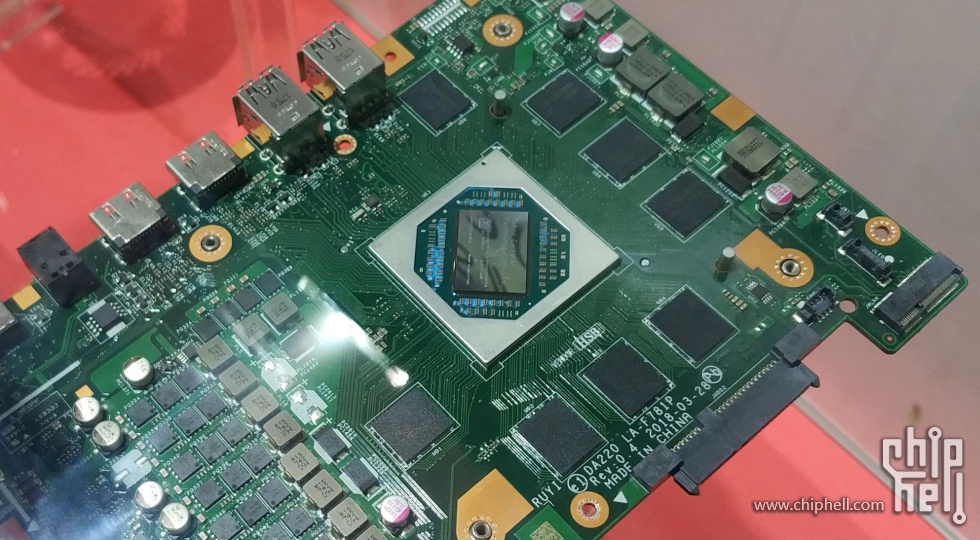
Is it a single chip or are the CPU & GPU separated?
Is it a single chip or are the CPU & GPU separated?
Single chip, it's a custom SoC. One Zen CCX is tiny anyway.
The "computer version" (or whatever was pictured here: http://nb.zol.com.cn/694/6949856.html ) uses Windows 10, and I think I saw it mentioned somewhere that console version would use "customized Win10"RAM is 256-bit on board, not on package as the Anandtech article clarified. I'm guessing their custom OS will be Linux.
And why does it look like the designer punched a PS4 Pro and called it a day?
What's the difference these days? OS?
D
Deleted member 11852
Guest
Wow, that's a beautiful board, even better than the ps4s.
Electrical engineer here. That board looks like a nightmare. That many components suggests it was either designed by three different people who never spoke to one another or was made to be costed to shave a dozen 1/100th dollar savings over the entire project. When you prioritise cost and disregard the impact on complexity, what you lose is reliability.
What's that army of grey squares on the left for? Never seen the like before.
Do note that it is only the "version 0.4" of the motherboard, final could be cleanerElectrical engineer here. That board looks like a nightmare. That many components suggests it was either designed by three different people who never spoke to one another or was made to be costed to shave a dozen 1/100th dollar savings over the entire project. When you prioritise cost and disregard the impact on complexity, what you lose is reliability.
What's that army of grey squares on the left for? Never seen the like before.
mosfets like these and inductors
Tkumpathenurple
Veteran
You will get 8 cores and you will be happy
Question is will we get 16 threads or not.
I've read suggestions that SMT wouldn't be useful for games, but would be suitable for the OS. If so, could that mean all 8 cores would be available for games, or does SMT have too much impact on clockspeeds?
I've read suggestions that SMT wouldn't be useful for games, but would be suitable for the OS. If so, could that mean all 8 cores would be available for games, or does SMT have too much impact on clockspeeds?
It's useful for most properly multi-threaded games, it's not useful only when your code treats an SMT thread like a physical CPU core and leaves other available CPU cores underutilized. This should never be an issue on consoles, and I see no reason not to include SMT.
You mean the power delivery? Yeah it's the only area I don't like, but while it looks "complex", it's just using more low-current, low temperature, discrete vrms, instead of very few high current ones. The design itself looks straightforward.Electrical engineer here. That board looks like a nightmare. That many components suggests it was either designed by three different people who never spoke to one another or was made to be costed to shave a dozen 1/100th dollar savings over the entire project. When you prioritise cost and disregard the impact on complexity, what you lose is reliability.
I don't know, between highend vrms like the ps4, versus many small ones, there is a big list of compromises to choose from with heat, emi, reliability, efficiency, cost... Heat and high current are lower reliability, number of parts are lower reliability, choose your poison.
They would follow guidelines from AMD for power delivery.
It might indicate a high clock... Or a prototype where they will shave off phases once they characterized everything.
Each slice is a VRM phase. From left to right... Input cap is the round metal can, three mosfets/vrm, and a grey inductor. Then the two black output caps filter all the phases together. There must be a couple vrm controllers on the left, or under, which we can't see.What's that army of grey squares on the left for? Never seen the like before.
So the gpu/cpu/memory are powered by 10 phases. Launch ps4 had 6 for cpu/gpu plus 2 for memory. There's a missing input cap, and two missing output caps (black rectangular), which could means they are going to remove those entire phases in the final version (or instead populate them?). There are probably more output caps under the board.
Seriously, outside of the discrete instead of integrated vrms, it has ridiculously little glue logic. I am guessing there's also a tranceiver chip for each connector under the board, right behind each connector, and some bios and board controller somewhere we can't see. ALL peripherals seem to be on the SoC.
https://arstechnica.com/information...rm-shuts-down-key-iphone-supplier-for-2-days/
So TSMC went and installed some new gear that came with a bonus WannaCry surprise, not likely to be relevant to next-gen consoles but it highlights how pervasive old busted tech is in even the most advanced industrial processes ffs Stop Using SMB1
So TSMC went and installed some new gear that came with a bonus WannaCry surprise, not likely to be relevant to next-gen consoles but it highlights how pervasive old busted tech is in even the most advanced industrial processes ffs Stop Using SMB1
- Status
- Not open for further replies.
Similar threads
- Replies
- 58
- Views
- 10K
- Replies
- 6
- Views
- 436
- Replies
- 37
- Views
- 3K

