
The japanese site pc.watch.impress.co.jp released a new article about the Xbox360 GPU.
Multiple threading Xbox 360 GPU which is designed to prerequisite
http://pc.watch.impress.co.jp/docs/2005/0914/kaigai212.htm
This is the translation from http://babelfish.altavista.com/
---------------
- GPU which has 24,576 these vectoring registers
The die/di of Xbox 360 GPU (the semiconductor itself) as for the air being attached directly with the photograph, the enormous SRAM area which scatters on the die/di. SRAM scatters in addition to the large area which is presumed cash the various parts without the ま difficult. To tell the truth this, the majority is the register.
Xbox 360 GPU has 24,576 these vectoring registers at total. Why, it seems that exceeds 2 ten thousand, that when you say, whether it has registers of a quantity which does not have either the way that is for multiple threading. For supporting the hardware multithread operation, the physical register for state change becomes enormously necessary. Because of that, with Xbox 360 GPU, you say that it has the enormous register.
As the compensation, with Xbox 360 GPU, cash quantity is economized. There is also GPU which considerably has large-sized cash in up-to-date GPU, but in case of Xbox 360 GPU you say that apex cash (Vertex Cache:VC) 8KB and texture cash (Texture Cache:TC) only the quantity of 32KB and minimum it is on-board. According to Microsoft, you say that the fact that, is the idea of basic Xbox 360 GPU, almost it does not depend on cash, with memory access threads.
One of the reasons where Xbox 360 GPU takes such design, is presumed that it is because of quality of the workload of GPU. In case of GPU, cash hit ratio it is low in comparison with CPU, on the other hand, there is a parallel conversion possible workload countlessly. Because of that, rather than increasing cash, the one which turns the resource of the amount to multiple threading becomes efficient. Entering into the memory access of long レイテンシ, if it threads, it can conceal ray ten シ. While if waiting for the fetch of the data, because another thread should have been executed just is. As for this with trend of the whole GPU, not only ATI Technologies which developed Xbox 360 GPU, also NVIDIA GeForce 6800 (NV40) later is opposite to multiple threading.
This can also think, from the point of view you use SRAM somewhere. Cash hit is high, to multithread operation with CPU where the workload which can be converted is little uses SRAM in cash. Vis-a-vis that, GPU which is the software environment of opposite uses SRAM in the register. 24,576 these 128bit vectoring registers, when it converts, become 384KB. In other words, SRAM of 400KB weak amount, with Xbox 360 instead of making cash it is the case that it turns to the register. Even with the same SRAM, the register the die/di area (the area on the semiconductor chip) takes from cash where the numbers of ports are few. Using the sufficient area which can place many cash, it means to arrange the register.
Unified-Shader of Xbox 360 GPU has total 48 the operational unit which is (ALU). As for respective ALU, the 4way vectoring unit of 128bit has 1 and 1way scalar unit 1 of 32bit inside. Are simultaneously order issue and processing possible vis-a-vis both units. Concerning each ALU, it becomes the calculation where these at a time 512 registers exist, but the register group is done share.
- 94 threads with on-the-fly hardware control
According to the information which Microsoft makes clear, Xbox 360 GPU can manage the maximum of 94 threads with the on-the-fly, you say that it has hardware multiple threading ability. This differs the number to which ATI reveals at the time of E3 (64 threads) with, but it is thought that it is the number where this is correct. As for the inside reason of threading, apex thread 31, pixel thread 63. 2 you express both and, start and power have become number minus 1.
Furthermore, as for the apex thread 64 apexes, as for the pixel thread it handles 64 pixels does the change of the state as one thread unit. In other words, as for 1 thread the processing for the apex 64, or, the processing for 64 pixels it is the case that it is formed to the upper limit. ATI, means to judge that this grain size is most appropriate. By the way, the GPU authorized personnel where expression of this differs depending upon the GPU vendor, calls each pixel 1 thread it is.
In case of GPU, it is not necessary for programmer side to do multithread operation programming. Instance is formed automatically from the parent thread. For example, the primitive is disassembled to the pixel which is processed with same シェーダ with the luster riser. With Xbox 360 GPU, binding the instance which is formed, it seems that it handles as 1 thread.
In addition, Xbox 360 GPU, other than hardware change of the thread, at the higher rank supports also the change of the context of GPU itself with the hardware. You can keep to maximum of 8 contexts with the hardware. Because of that, シェーダ every is changed, the former way, it is not necessary the flash to do the GPU pipe. As for the GPU pipe because it is long, when the flash it does once, penalty is very large. But, if Xbox 360 GPU because context of 8 aspects is kept, it can designate the change of the state low as cost.

- As for テッセレータhardware mounting
When it keeps seeing the GPU pipe from above, "command processor (Command Processor:CP)" reads out command first from the command buffer with respect to main memory. "The apex glue per (Vertex Grouper)" under that, plane surface division is done, "ハードウェアテッセレータ(Hardware Tessellator)" has belonged. "Vertex Grouper & Tessellator (VGT)" with it has become the name which is said.
As for Microsoft, as for Tessellator of Xbox 360 GPU, you say that in the consumer machine it is Tessellator of new practical efficiency. In the past, using Shader array with this corner, you wrote the estimate that it does テッセレート, but so was not. The apex which テッセレート is done is output of 1 apex/cycle, but テッセレーテッド apex because it is easy to be recorded before cash, calls the lowness of throughput that it is concealed probably will be.
As for シェーダユニット with Unified-Shader type, there is no distinction of Vertex Shader and Pixel Shader the former way. With Xbox 360 GPU the sequencer (Sequencer) executes control flow order, does the control of each Shader array. The Shader array group and it is the image the combination of Sequencer of Shader. Because of that, in the figure where Microsoft this time shows, as for Shader array it was expressed ALU.
The ALU group of Shader is divided into 3 banks. Control of multiple threading is done at this bank unit. Shader フィーチャ Programable Shader of DirectX becomes 3.0 plus something. In other words, internal operational precision becomes 32bit, furthermore function is expanded.
As for texture pipe, texture Sanplatinum 16 units. When 48 you call you compare with the quantity of Shader ALU, it is little, the sea urchin it is visible, but this is presumed the for the sake of perhaps GPU is designed in multiple threading subject. Hardware threading is not done, (or width of threading is narrow) when, as much as possible to be quick it is necessary to fetch texture. Because of that, making the texture pipe thick, you must hold down the delay due to competition as little as possible.
But, at the time of cash mistake if it threads, until the texture data is loaded, be sure to be possible to be able to make wait ALU side. Because レイテンシ may become long, it can hold down the texture pipe to a last quantity which can maintain throughput.
- Outputting the processing result of Shader freely
"シェーダエクスポート (Shader Export:SX)" with it is called under Shader ALU array, there is a unique unit. Shader Export as in name with the unit which manages the output from Shader, does the processing only of Unified-Shader which does not have the distinction of Vertex Shader and Pixel Shader.
The apex data with Shader apex after shading, "the primitive assembler (Primitive Assember A)" to with is output from this Shader Export. "The scan converter (Scan Converter:SC)" with being rasterized from there, disassembly to pixel. After that, again it is reset by Shader array, pixel shading is done.
"Backend Central (BC)" with there is the block which is called under Shader Export, this has administered the data transfer of eDRAM and the processing etc. which outputs the processing result to main memory. The pixel data which is output from Shader is usually sent to the pixel processing block inside GPU. But, in case of Xbox 360 GPU, it is sent to eDRAM via Backend Central. Then, the processing of Alpha, Z and the stencil is done, the processing result is reset to Backend Central lastly.
Two dice/di of eDRAM and GPU (the semiconductor itself), the private interface whose bus width is wide on the baseplate of the package (HSIO) with it is tied. As for zone between both tip/chip 32GB/sec. It is the zone which is agreeable to the case where with 16GB/sec rendering it does this, in eDRAM, with 16GB/sec writes resets on GPU main die/di side and exactly. Because the memory hub (MH) to zone is 16GB/sec from the GPU core, 32GB/sec is seen that it is necessary. By the way, Z/Alpha processor group and eDRAM of the eDRAM die/di are tied with the wide band of 256GB/sec. Among processing of the whole GPU, just the processing which eats memory zone is the idea using eDRAM.
But, because the capacity of eDRAM it is 10MB, when 720p of HDTV resolution (the 1,280×720 dot) with it designates as MSAA, it becomes insufficient. Because of that, divided rendering is done. You say that it supports divided rendering itself, with the hardware, and the library tries not to be visible from program side. In divided rendering, because as for the geometry which extends over the divided line it is necessary to draw doubly, as for apex processing it becomes the overhead of approximately 1.2 - 1.3 times, (pixel processing side the overhead says is not) with.
With Xbox 360 GPU, in order to do fixing pixel processing with eDRAM, for PC like GPU it is not necessary to save video memory zone. Because of that, compression of the color and the Z data is not done in the pipeline. It means that the compressed of color &Z/extension circuit was excluded.
The function which anticipates the next generation Shader is added to Xbox 360 GPU. The direct data to memory it writes out the one of them, from シェーダ in the pipeline which joins with DirectX 10 of the next generation "シェーダメモリエクスポート (Shader Memory Export)" is. With Xbox 360 GPU, direct output can designate the result which is calculated with Shader, as optional address in memory. As for this, in order to do general-purpose processing with GPU, it is said that it is the function which cannot be missed.
As for the pixel output of Xbox 360 GPU, with color &Z 8 pixels/cycle. Z if only being to be half, it becomes 16 pixels/cycle. The filtering itself of MSAA is not eDRAM side, it does with Backend Central block of main die/di side.
- As for the die/di size of Xbox 360 GPU approximately 200 squares mm?
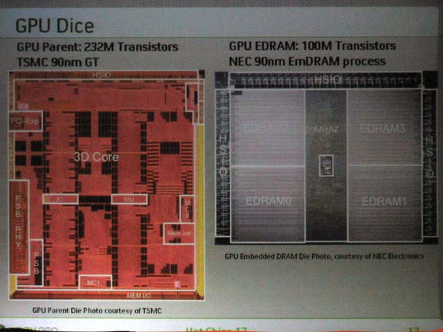
As for Microsoft, as for the die/di size of Xbox 360 GPU it is not open. As for the number of transistors, GPU main die/di 232M (2 hundred million 3,200 ten thousand), eDRAM 100M (1 hundred million). The main die/di RADEON X800 (R420/423) 160M of system (1 hundred million 6,000 ten thousand) is approximately 50% increase of the transistor, but because production process becomes 90nm, die/di size (the area of the semiconductor itself) it is seen that it reduces. In regard to calculation it becomes approximately 200 squares mm. With Web, in 200 squares mm or less it was visible even with the package photograph which leak is done.
When for PC the die/di of high end GPU exceeds 300 squares mm, when you compare, with small inclination, it is GPU of PLAYSTATION 3, "RSX (Reality Synthesizer)" with in comparison it is presumed that it is small. But, with Xbox 360 GPU, because eDRAM which belongs perhaps with 70 squares mm, it becomes the multichip module which places 2 dice/di, as for cost of altogether GPU it is not low under any condition. The die/di of XGPU of Xbox of the first generation with approximately 150 squares mm or less, was small directly.
As ahead this, process technology advances, both dice/di shrink. As for Microsoft for decreasing cost, the necessity perhaps to integrate the GPU die/di and the eDRAM die/di probably will arise. In that case, there is the challenge that it changes the production process technology of GPU itself into DRAM mixed loading process.
When the information which has become anew clear is synthesized, the form of Xbox 360 GPU more and more becomes clear. Xbox 360 GPU, was designed to multiple threading subject with GPU of new directivity, Unified-Shader type architecture has matched to the design philosophy. In addition, by the fact that eDRAM is used, it decreases the pressure to memory zone, it has succeeded in excluding color &Z compressed function and the like. As for Xbox 360 GPU, the quantities of Shader ALU 48 the number of many transistors are few comparatively, but also the reason may be hidden in this.

Multiple threading Xbox 360 GPU which is designed to prerequisite
http://pc.watch.impress.co.jp/docs/2005/0914/kaigai212.htm
This is the translation from http://babelfish.altavista.com/
---------------
- GPU which has 24,576 these vectoring registers
The die/di of Xbox 360 GPU (the semiconductor itself) as for the air being attached directly with the photograph, the enormous SRAM area which scatters on the die/di. SRAM scatters in addition to the large area which is presumed cash the various parts without the ま difficult. To tell the truth this, the majority is the register.
Xbox 360 GPU has 24,576 these vectoring registers at total. Why, it seems that exceeds 2 ten thousand, that when you say, whether it has registers of a quantity which does not have either the way that is for multiple threading. For supporting the hardware multithread operation, the physical register for state change becomes enormously necessary. Because of that, with Xbox 360 GPU, you say that it has the enormous register.
As the compensation, with Xbox 360 GPU, cash quantity is economized. There is also GPU which considerably has large-sized cash in up-to-date GPU, but in case of Xbox 360 GPU you say that apex cash (Vertex Cache:VC) 8KB and texture cash (Texture Cache:TC) only the quantity of 32KB and minimum it is on-board. According to Microsoft, you say that the fact that, is the idea of basic Xbox 360 GPU, almost it does not depend on cash, with memory access threads.
One of the reasons where Xbox 360 GPU takes such design, is presumed that it is because of quality of the workload of GPU. In case of GPU, cash hit ratio it is low in comparison with CPU, on the other hand, there is a parallel conversion possible workload countlessly. Because of that, rather than increasing cash, the one which turns the resource of the amount to multiple threading becomes efficient. Entering into the memory access of long レイテンシ, if it threads, it can conceal ray ten シ. While if waiting for the fetch of the data, because another thread should have been executed just is. As for this with trend of the whole GPU, not only ATI Technologies which developed Xbox 360 GPU, also NVIDIA GeForce 6800 (NV40) later is opposite to multiple threading.
This can also think, from the point of view you use SRAM somewhere. Cash hit is high, to multithread operation with CPU where the workload which can be converted is little uses SRAM in cash. Vis-a-vis that, GPU which is the software environment of opposite uses SRAM in the register. 24,576 these 128bit vectoring registers, when it converts, become 384KB. In other words, SRAM of 400KB weak amount, with Xbox 360 instead of making cash it is the case that it turns to the register. Even with the same SRAM, the register the die/di area (the area on the semiconductor chip) takes from cash where the numbers of ports are few. Using the sufficient area which can place many cash, it means to arrange the register.
Unified-Shader of Xbox 360 GPU has total 48 the operational unit which is (ALU). As for respective ALU, the 4way vectoring unit of 128bit has 1 and 1way scalar unit 1 of 32bit inside. Are simultaneously order issue and processing possible vis-a-vis both units. Concerning each ALU, it becomes the calculation where these at a time 512 registers exist, but the register group is done share.
- 94 threads with on-the-fly hardware control
According to the information which Microsoft makes clear, Xbox 360 GPU can manage the maximum of 94 threads with the on-the-fly, you say that it has hardware multiple threading ability. This differs the number to which ATI reveals at the time of E3 (64 threads) with, but it is thought that it is the number where this is correct. As for the inside reason of threading, apex thread 31, pixel thread 63. 2 you express both and, start and power have become number minus 1.
Furthermore, as for the apex thread 64 apexes, as for the pixel thread it handles 64 pixels does the change of the state as one thread unit. In other words, as for 1 thread the processing for the apex 64, or, the processing for 64 pixels it is the case that it is formed to the upper limit. ATI, means to judge that this grain size is most appropriate. By the way, the GPU authorized personnel where expression of this differs depending upon the GPU vendor, calls each pixel 1 thread it is.
In case of GPU, it is not necessary for programmer side to do multithread operation programming. Instance is formed automatically from the parent thread. For example, the primitive is disassembled to the pixel which is processed with same シェーダ with the luster riser. With Xbox 360 GPU, binding the instance which is formed, it seems that it handles as 1 thread.
In addition, Xbox 360 GPU, other than hardware change of the thread, at the higher rank supports also the change of the context of GPU itself with the hardware. You can keep to maximum of 8 contexts with the hardware. Because of that, シェーダ every is changed, the former way, it is not necessary the flash to do the GPU pipe. As for the GPU pipe because it is long, when the flash it does once, penalty is very large. But, if Xbox 360 GPU because context of 8 aspects is kept, it can designate the change of the state low as cost.

- As for テッセレータhardware mounting
When it keeps seeing the GPU pipe from above, "command processor (Command Processor:CP)" reads out command first from the command buffer with respect to main memory. "The apex glue per (Vertex Grouper)" under that, plane surface division is done, "ハードウェアテッセレータ(Hardware Tessellator)" has belonged. "Vertex Grouper & Tessellator (VGT)" with it has become the name which is said.
As for Microsoft, as for Tessellator of Xbox 360 GPU, you say that in the consumer machine it is Tessellator of new practical efficiency. In the past, using Shader array with this corner, you wrote the estimate that it does テッセレート, but so was not. The apex which テッセレート is done is output of 1 apex/cycle, but テッセレーテッド apex because it is easy to be recorded before cash, calls the lowness of throughput that it is concealed probably will be.
As for シェーダユニット with Unified-Shader type, there is no distinction of Vertex Shader and Pixel Shader the former way. With Xbox 360 GPU the sequencer (Sequencer) executes control flow order, does the control of each Shader array. The Shader array group and it is the image the combination of Sequencer of Shader. Because of that, in the figure where Microsoft this time shows, as for Shader array it was expressed ALU.
The ALU group of Shader is divided into 3 banks. Control of multiple threading is done at this bank unit. Shader フィーチャ Programable Shader of DirectX becomes 3.0 plus something. In other words, internal operational precision becomes 32bit, furthermore function is expanded.
As for texture pipe, texture Sanplatinum 16 units. When 48 you call you compare with the quantity of Shader ALU, it is little, the sea urchin it is visible, but this is presumed the for the sake of perhaps GPU is designed in multiple threading subject. Hardware threading is not done, (or width of threading is narrow) when, as much as possible to be quick it is necessary to fetch texture. Because of that, making the texture pipe thick, you must hold down the delay due to competition as little as possible.
But, at the time of cash mistake if it threads, until the texture data is loaded, be sure to be possible to be able to make wait ALU side. Because レイテンシ may become long, it can hold down the texture pipe to a last quantity which can maintain throughput.
- Outputting the processing result of Shader freely
"シェーダエクスポート (Shader Export:SX)" with it is called under Shader ALU array, there is a unique unit. Shader Export as in name with the unit which manages the output from Shader, does the processing only of Unified-Shader which does not have the distinction of Vertex Shader and Pixel Shader.
The apex data with Shader apex after shading, "the primitive assembler (Primitive Assember
A)" to with is output from this Shader Export. "The scan converter (Scan Converter:SC)" with being rasterized from there, disassembly to pixel. After that, again it is reset by Shader array, pixel shading is done."Backend Central (BC)" with there is the block which is called under Shader Export, this has administered the data transfer of eDRAM and the processing etc. which outputs the processing result to main memory. The pixel data which is output from Shader is usually sent to the pixel processing block inside GPU. But, in case of Xbox 360 GPU, it is sent to eDRAM via Backend Central. Then, the processing of Alpha, Z and the stencil is done, the processing result is reset to Backend Central lastly.
Two dice/di of eDRAM and GPU (the semiconductor itself), the private interface whose bus width is wide on the baseplate of the package (HSIO) with it is tied. As for zone between both tip/chip 32GB/sec. It is the zone which is agreeable to the case where with 16GB/sec rendering it does this, in eDRAM, with 16GB/sec writes resets on GPU main die/di side and exactly. Because the memory hub (MH) to zone is 16GB/sec from the GPU core, 32GB/sec is seen that it is necessary. By the way, Z/Alpha processor group and eDRAM of the eDRAM die/di are tied with the wide band of 256GB/sec. Among processing of the whole GPU, just the processing which eats memory zone is the idea using eDRAM.
But, because the capacity of eDRAM it is 10MB, when 720p of HDTV resolution (the 1,280×720 dot) with it designates as MSAA, it becomes insufficient. Because of that, divided rendering is done. You say that it supports divided rendering itself, with the hardware, and the library tries not to be visible from program side. In divided rendering, because as for the geometry which extends over the divided line it is necessary to draw doubly, as for apex processing it becomes the overhead of approximately 1.2 - 1.3 times, (pixel processing side the overhead says is not) with.
With Xbox 360 GPU, in order to do fixing pixel processing with eDRAM, for PC like GPU it is not necessary to save video memory zone. Because of that, compression of the color and the Z data is not done in the pipeline. It means that the compressed of color &Z/extension circuit was excluded.
The function which anticipates the next generation Shader is added to Xbox 360 GPU. The direct data to memory it writes out the one of them, from シェーダ in the pipeline which joins with DirectX 10 of the next generation "シェーダメモリエクスポート (Shader Memory Export)" is. With Xbox 360 GPU, direct output can designate the result which is calculated with Shader, as optional address in memory. As for this, in order to do general-purpose processing with GPU, it is said that it is the function which cannot be missed.
As for the pixel output of Xbox 360 GPU, with color &Z 8 pixels/cycle. Z if only being to be half, it becomes 16 pixels/cycle. The filtering itself of MSAA is not eDRAM side, it does with Backend Central block of main die/di side.
- As for the die/di size of Xbox 360 GPU approximately 200 squares mm?
As for Microsoft, as for the die/di size of Xbox 360 GPU it is not open. As for the number of transistors, GPU main die/di 232M (2 hundred million 3,200 ten thousand), eDRAM 100M (1 hundred million). The main die/di RADEON X800 (R420/423) 160M of system (1 hundred million 6,000 ten thousand) is approximately 50% increase of the transistor, but because production process becomes 90nm, die/di size (the area of the semiconductor itself) it is seen that it reduces. In regard to calculation it becomes approximately 200 squares mm. With Web, in 200 squares mm or less it was visible even with the package photograph which leak is done.
When for PC the die/di of high end GPU exceeds 300 squares mm, when you compare, with small inclination, it is GPU of PLAYSTATION 3, "RSX (Reality Synthesizer)" with in comparison it is presumed that it is small. But, with Xbox 360 GPU, because eDRAM which belongs perhaps with 70 squares mm, it becomes the multichip module which places 2 dice/di, as for cost of altogether GPU it is not low under any condition. The die/di of XGPU of Xbox of the first generation with approximately 150 squares mm or less, was small directly.
As ahead this, process technology advances, both dice/di shrink. As for Microsoft for decreasing cost, the necessity perhaps to integrate the GPU die/di and the eDRAM die/di probably will arise. In that case, there is the challenge that it changes the production process technology of GPU itself into DRAM mixed loading process.
When the information which has become anew clear is synthesized, the form of Xbox 360 GPU more and more becomes clear. Xbox 360 GPU, was designed to multiple threading subject with GPU of new directivity, Unified-Shader type architecture has matched to the design philosophy. In addition, by the fact that eDRAM is used, it decreases the pressure to memory zone, it has succeeded in excluding color &Z compressed function and the like. As for Xbox 360 GPU, the quantities of Shader ALU 48 the number of many transistors are few comparatively, but also the reason may be hidden in this.


