Intel CPU Transistor Density : 90 nm generation...

From Anandtech's IDF coverage
prescottdie.jpg

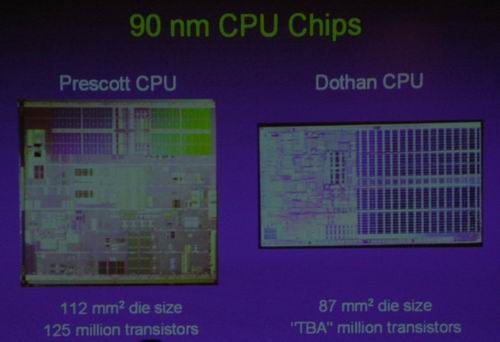
Of two new 90 nm Intel CPUs, of the particular interest to us is Dothan, which packs in more transistors(150 million??) than Prescott(125 million transistors) due to its 2MB L2 cache. What's even more incredible is that Dothan achieves 3X transistor density of SCEI's PSX2OAC, which weights in 55 million transistors on same die size.

Intel's fab technolgy is clearly superior to SCEI/Toshiba's, yet Intel is not talking about putting 4 Pentium4s in single die in next 65 nm generation....(Dual-core is a possibility). So why are you Sony fans expecting to see quad-CELLcores in your PSX3....
 
Intel's fab technolgy is clearly superior to SCEI/Toshiba's, yet Intel is not talking about putting 4 Pentium4s in single die in next 65 nm generation....(Dual-core is a possibility). So why are you Sony fans expecting to see quad-CELLcores in your PSX3....

Who has the world's fastest and smallest transistor(with 30nm yet faster than even intel's 20nm trans in the lab)? Who's got neato tech from many a people(making it easier to pack more embbdded stuff, etc.)? Who's making a Tflops level chip?

ed

PS If anything that helps demonstrate the viability of 500M+ trans chips at 65nm.
 
...

PS If anything that helps demonstrate the viability of 500M+ trans chips at 65nm.
Sure, if the CPU is 90% SRAM and carries very little logic.. It will have a massive gate density per mm2 but its FLOP rating won't be anything to write home about.

BTW, I read that Intel did confirm the rumor that Prescott will burn more than 100 W. At this rate, your PCs are going to double as room heaters and coffee makers....
 
Re: ...

DeadmeatGA said:
BTW, I read that Intel did confirm the rumor that Prescott will burn more than 100 W. At this rate, your PCs are going to double as room heaters and coffee makers....

I heard it will be more like 120W. I see an X-Box 2 burning 200W or more. ;)

Fredi
 
DeadmeatGA said:
Intel's fab technolgy is clearly superior to SCEI/Toshiba's, yet Intel is not talking about putting 4 Pentium4s in single die in next 65 nm generation....(Dual-core is a possibility). So why are you Sony fans expecting to see quad-CELLcores in your PSX3....

It seems like Intel is more focused on multithreading, than true parallel processing?
 
Re: ...

DeadmeatGA said:
Sure, if the CPU is 90% SRAM and carries very little logic.. It will have a massive gate density per mm2 but its FLOP rating won't be anything to write home about.

(bangs head on wall)

Ok. Hmm. A chip that devotes 90% of it's area to SRAM will have a lower aggregate density than one that utilizes, say, eDRAM (by a factor of ~6 IIRC). How is that "massive" in terms of density?

Next. IBM stated in a presentation that for the 65nm node, you can yeild a gate density (K gates per sq. mm) of 680.

Even if you devote, say, 10mm^2 of your die to logic and factor in area 'tradeoffs' due to design - you're nearing 50Million logic gates, or over half a billion tranistsors (with the theoretical bound set at 68M gates). And we're talking of an IC that's an aggregate 250+mm^2.

And finally. You keep making an ass out of yourself by compering a superscalar CPU's "Flops rating" with that which will be achieved by [more] dedicated logic that's present in a horizonal plurality. Cell will be much more akin to a DX10 (probobly much higher level) GPU's architecture. It has a massive bias towards concurrency in way of FP/Vec computations. And when you look at GPU's you'll see - as some already stated (whom ever you are just raise your hand) - that they're already crunching well, well over a trillion ops a second, with a 'Flops' rating that's well over 200 (eg. NV3x is like ~200 and I'm sure the R3xx core has it beat).

There is nothing in this design that's impossible.
 
DeadmeatGA said:
From Anandtech's IDF coverage
prescottdie.jpg

Of two new 90 nm Intel CPUs, of the particular interest to us is Dothan, which packs in more transistors(150 million??) than Prescott(125 million transistors) due to its 2MB L2 cache. What's even more incredible is that Dothan achieves 3X transistor density of SCEI's PSX2OAC, which weights in 55 million transistors on same die size.

Intel's fab technolgy is clearly superior to SCEI/Toshiba's, yet Intel is not talking about putting 4 Pentium4s in single die in next 65 nm generation....(Dual-core is a possibility). So why are you Sony fans expecting to see quad-CELLcores in your PSX3....

Intel sucks... look their competitor is making a 90 nm chip called Dothan that in 87 mm^2 packs more transistors than Prescott does in 112 mm^2...

Wait, I must have suffered of Deadmeat-ism: ever thought that EE+GS@90 nm ( packing more e-DRAM they could boast the transistor count by quite a bit without needing many more mm^2 of surfce area ) is not the peak that SCE, Toshiba and IBM can do with their 90 nm, 65 nm and 45 nm nodes ?

I can't wait when Toshiba gives up even fresher updates on their capacitor-less e-DRAM ( say thanks to SOI :) ) that should see use in CELL products in the 45 nm generation: that will make for VERY small e-DRAM cells.
 
Panajev2001a said:
DeadmeatGA said:
Intel sucks... look their competitor is making a 90 nm chip called Dothan that in 87 mm^2 packs more transistors than Prescott does in 112 mm^2...

:LOL::LOL::LOL::LOL::LOL:

You're joking, right?


McFly said:
DeadmeatGA said:
BTW, I read that Intel did confirm the rumor that Prescott will burn more than 100 W. At this rate, your PCs are going to double as room heaters and coffee makers....


I heard it will be more like 120W. I see an X-Box 2 burning 200W or more.

That's why I'm apt to believe that the XB2 will use a Pentium M or Athlon 64. More on the latter as it's more powerful and has dual-core capabilities.
 
Panajev2001a said:
DeadmeatGA said:
From Anandtech's IDF coverage
prescottdie.jpg

Of two new 90 nm Intel CPUs, of the particular interest to us is Dothan, which packs in more transistors(150 million??) than Prescott(125 million transistors) due to its 2MB L2 cache. What's even more incredible is that Dothan achieves 3X transistor density of SCEI's PSX2OAC, which weights in 55 million transistors on same die size.

Intel's fab technolgy is clearly superior to SCEI/Toshiba's, yet Intel is not talking about putting 4 Pentium4s in single die in next 65 nm generation....(Dual-core is a possibility). So why are you Sony fans expecting to see quad-CELLcores in your PSX3....

Intel sucks... look their competitor is making a 90 nm chip called Dothan that in 87 mm^2 packs more transistors than Prescott does in 112 mm^2...

Wait, I must have suffered of Deadmeat-ism: ever thought that EE+GS@90 nm ( packing more e-DRAM they could boast the transistor count by quite a bit without needing many more mm^2 of surfce area ) is not the peak that SCE, Toshiba and IBM can do with their 90 nm, 65 nm and 45 nm nodes ?

I can't wait when Toshiba gives up even fresher updates on their capacitor-less e-DRAM ( say thanks to SOI :) ) that should see use in CELL products in the 45 nm generation: that will make for VERY small e-DRAM cells.

What do you think ? :LOL:
 
nonamer said:
Panajev2001a said:
DeadmeatGA said:
Intel sucks... look their competitor is making a 90 nm chip called Dothan that in 87 mm^2 packs more transistors than Prescott does in 112 mm^2...

:LOL::LOL::LOL::LOL::LOL:

You're joking, right?


McFly said:
DeadmeatGA said:
BTW, I read that Intel did confirm the rumor that Prescott will burn more than 100 W. At this rate, your PCs are going to double as room heaters and coffee makers....


I heard it will be more like 120W. I see an X-Box 2 burning 200W or more.

That's why I'm apt to believe that the XB2 will use a Pentium M or Athlon 64. More on the latter as it's more powerful and has dual-core capabilities.
They are just going to go for an under volted lower clocked version of whatever the fastest chip is at the time. Its the gpu that they have to be worried about .
 
jvd said:
They are just going to go for an under volted lower clocked version of whatever the fastest chip is at the time. Its the gpu that they have to be worried about .

Actually, MS choose the P3 over the Athlons because it was cooler, even though the Athlon's were faster. At 100W+ heat output, the Prescott/Tejas may be completely unacceptable, no matter how underclocked it is. My bet is that they simply won't go for an chip w/o good heat management.
 
nonamer said:
jvd said:
They are just going to go for an under volted lower clocked version of whatever the fastest chip is at the time. Its the gpu that they have to be worried about .

Actually, MS choose the P3 over the Athlons because it was cooler, even though the Athlon's were faster. At 100W+ heat output, the Prescott/Tejas may be completely unacceptable, no matter how underclocked it is. My bet is that they simply won't go for an chip w/o good heat management.
Yes but that is the top of the line chips on .13 micron that was supposed to be relased now but was delayed and now we have the xeons rebranded extreme edition to go against the a64 fx. The thing is if you shave off 500mhz - 1ghz and drop the voltage of the chip from say 1.7-1.5 or less you will notice huge tempeture decreases. If you have an unlocked athlon or an athlon with a nforce 2 lower the vcore and the multiplyer and watch how quickly the heat drops . If i drop my 3200 down 300mhz and move the voltage down .3 I notice a 10 degree diffrence. Which brings it down to 4cabove room temp with case temp 2c above room temp.

With the prescotts they can do the same as long as they don't want the top of the line cpu speed. Which i have never know them to want .
 
jvd said:
nonamer said:
jvd said:
They are just going to go for an under volted lower clocked version of whatever the fastest chip is at the time. Its the gpu that they have to be worried about .

Actually, MS choose the P3 over the Athlons because it was cooler, even though the Athlon's were faster. At 100W+ heat output, the Prescott/Tejas may be completely unacceptable, no matter how underclocked it is. My bet is that they simply won't go for an chip w/o good heat management.
Yes but that is the top of the line chips on .13 micron that was supposed to be relased now but was delayed and now we have the xeons rebranded extreme edition to go against the a64 fx. The thing is if you shave off 500mhz - 1ghz and drop the voltage of the chip from say 1.7-1.5 or less you will notice huge tempeture decreases. If you have an unlocked athlon or an athlon with a nforce 2 lower the vcore and the multiplyer and watch how quickly the heat drops . If i drop my 3200 down 300mhz and move the voltage down .3 I notice a 10 degree diffrence. Which brings it down to 4cabove room temp with case temp 2c above room temp.

With the prescotts they can do the same as long as they don't want the top of the line cpu speed. Which i have never know them to want .

It's not that simple. We're look at a 2x difference in heat between the Prescott (and possibly Tejas) versus the A64 and even more so for the P-M, but the performance is in the same ballpark. If the Prescott/Tejas were downclocked to actually match the A64 or P-M in heat, it would be woefully beatened. Likewise, the same could be done for the A64 (not really necessary for the P-M) and the next-gen P4's would have to be utterly crippled to keep up in this. Of course, they may be able to get leakage under control by 65nm, but the design of the Prescott and Tejas (Nehalem is a mystery though) is inherently hotter than a A64 or P-M. Besides, I'm always for the A64 because it has dual-core and 64-bit capabilities. For a console, that's hard to beat. ;)
 
yet Intel is not talking about putting 4 Pentium4s in single die in next 65 nm generation....(Dual-core is a possibility).

:) DM finally accepting multi-core huh ?

Intel does have plan for a 4 cores processors.

But you know Intel, they promote two core first and make alot of money on that, than 4 cores later. Its just a good business decision.


Here an old article a year ago on Intel discussing multi-core. There are alot more if you google around. You seems to miss alot.

http://zdnet.com.com/2100-1103-954456.html

"Multi-core is a very efficient way to use up transistors and increase performance," Brookwood said.
 
:idea: I wouldn't use Intel as a benchmark for transistor density, they want to produce their chips by the boatload and make a massive profit off of each one. Sony on the on the other hand won't mind getting poor yields and making a loss on each chip, for Intel this simply isn't an option. You should look at it like, "if Intel can do this much while making a substantial profit, imagine what Sony can do at a loss"
 
nonamer said:
It's not that simple. We're look at a 2x difference in heat between the Prescott (and possibly Tejas) versus the A64 and even more so for the P-M, but the performance is in the same ballpark. If the Prescott/Tejas were downclocked to actually match the A64 or P-M in heat, it would be woefully beatened. Likewise, the same could be done for the A64 (not really necessary for the P-M) and the next-gen P4's would have to be utterly crippled to keep up in this. Of course, they may be able to get leakage under control by 65nm, but the design of the Prescott and Tejas (Nehalem is a mystery though) is inherently hotter than a A64 or P-M.
Would you like to share some information on the power consumption of any Hammer-core CPU? Cause AMD isn't exactly forthcoming with it.

cu

incurable
 
incurable said:
Would you like to share some information on the power consumption of any Hammer-core CPU? Cause AMD isn't exactly forthcoming with it.

TDI (Thermal design power) for the Athlon FX platform is 85W. That is the guaranteed not to exceed limit for the highest end CPU to go in that form factor. So will probably be for a 2.2GHz or 2.4GHz CPU. Currently the 1.8GHz Opteron uses around 55W.

Cheers
Gubbi
 
Re: ...

Vince said:
DeadmeatGA said:
Sure, if the CPU is 90% SRAM and carries very little logic.. It will have a massive gate density per mm2 but its FLOP rating won't be anything to write home about.

(bangs head on wall)

Ok. Hmm. A chip that devotes 90% of it's area to SRAM will have a lower aggregate density than one that utilizes, say, eDRAM (by a factor of ~6 IIRC). How is that "massive" in terms of density?

Depends on wether you're measuring memory cell density (bits) or transistor density.

eDRAM obviously has higher bit density than SRAM. SRAM however has higher transistor density than eDRAM (6x transistors going into 3x the space).

Anyway. It's an apples to oranges comparison, so shouldn't be done. Compare logic devices to logic devices, SRAM cells to SRAM cells and eDRAM cells to eDRAM cells.

Cheers
Gubbi
 
Back
Top