Intel ARC GPUs, Xe Architecture for dGPUs [2018-2022]

Status
Not open for further replies.
Could these boards employ the much-publicized Omni-Directional Interconnect (ODI), which combines silicon interposer (Embedded Multi-Interconnect Bridge, EMIB) with 3D stacking (Foveros)?
https://www.extremetech.com/computi...irectional-interconnect-combines-emib-foveros
https://fuse.wikichip.org/news/2503...together-adds-omni-directional-interconnects/
https://fuse.wikichip.org/news/3508...l-3d-packaging-tech-gains-omnidirectionality/

AMD and NVIDIA are supposed to use the TMSC CoWoS interposer for HBM-based products.
ODI is very not soon(TM).
Also Co-EMIB is not ODI.
 
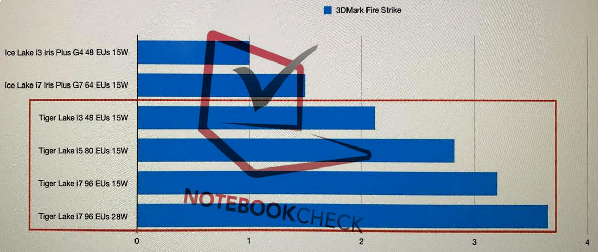
https://videocardz.com/newz/intel-tigerlake-gen12-xe-graphics-is-twice-as-fast-as-icelakes-gen11

Intel-Tiger-Lake-Gen12-Graphics-Performance.jpg
 
Those are excellent results, and they should give Renoir a hard time.

I wonder how the 48 EU Tiger Lake is being so much better than the 64 EU Ice Lake. Maybe they Xe EUs are wider?
 
Raja has posted photos of what appears to be 3 Seperate Xe -HP based GPUs.

We have seen the one on the left hand side before but the smaller one and larger ones are new.

Many are speculating that the larger one is a 4 Tile Arctic Sound GPU
EbVgsUeXsAAnpaI

And this picture here that Raja posted seems to prove that:
upload_2020-6-26_22-4-47.png
ATS = Arctic Sound
4T = 4 Tiles.

Raja also gave a vague hint on performance

Almost 1 PetaOps, many assume this is INT8.
 
256 TOPS per Arctic Sound chip.
If that's INT8, then 128 TFLOPs FP16, 64 TFLOPs FP32?

Naah, way too much. Unless it's using some dedicated tensor units and those are matrix operations like nvidia's hardware.
 
256 TOPS per Arctic Sound chip.
If that's INT8, then 128 TFLOPs FP16, 64 TFLOPs FP32?

Naah, way too much. Unless it's using some dedicated tensor units and those are matrix operations like nvidia's hardware.
They could very well have some tensor units in there, or some other means to run low precisions at much higher rate.
These chips fit nicely with the old leak too
upload_2020-6-27_5-11-3.png
 
https://newsroom.intel.com/press-kits/architecture-day-2020

All kinds of details, also gaming GPUs will be "Xe-HPG" and they'll be made at external foundry (read: TSMC)
In Xe-LP they've gone from Gen11's 4 FP/Int + 4 FP/ExtMath to 8 FP/Int + 2 ExtMath pipes and two EUs now share Thread controller. 6 texturing units capable of 48 texels/clock and 24 ROPs for 96 EUs

edit:
Also, Xe-HP FP32 FLOPS: 1 tile ~10.6 TFLOPS, 2 tiles ~21.2 TFLOPS (1.999x) and 4 tiles ~42,3 TFLOPS (3.993x). 512 EUs running at 1,3 GHz
 
All kinds of details, also gaming GPUs will be "Xe-HPG" and they'll be made at external foundry (read: TSMC)
Could be Samsung. TSMC will be for their CPU but OTOH they seem pretty full with orders.
 
I am not expecting the gaming chips (Xe-HPG) to provide any stellar or competitive performance with AMD or NVIDIA, since it relies on the same scalability scheme as Xe-HPC, ie: relies on racking up several tiles of graphics to scale up core count, this will be a mess for drivers and games in general.
 
No, those are single dies packed in organic carriers.
The actual IP is just subpar.
The architecture relies purely on software scoreboarding (software schedulers), which means Intel will have it's hands full writing good drivers for it to achieve good utilization (VLIW5 days anyone?), then on top of that they are scaling it up through tiling (multi core/die approach), which means it's going to be a nightmare to write drivers for, and to extract good performance from.

This is literally the laziest effort for making a new GPU in recent memory.
 
Removing scoreboarding from hardware enabled the power nightmare that was Fermi to become the somewhat efficient Kepler (among others of course). So, at least for the starting point, which is integrated graphics, that step totally makes sense. And Intel has a ton of software people (idk though if they are necessarily good at gfx driver compilers).
 
The architecture relies purely on software scoreboarding (software schedulers), which means Intel will have it's hands full writing good drivers for it to achieve good utilization (VLIW5 days anyone?)
Not really.
This is literally the laziest effort for making a new GPU in recent memory.
Nah, QC takes the cake.
And Intel has a ton of software people (idk though if they are necessarily good at gfx driver compilers).
Their s/w top talent is very much compiler people so this move isn't unwarranted.
Unfortunately the IP is still "meh" at best and they clearly lack focus.
Like dear god, what, 4 flavors of Gen12?
Why even.
 
Removing scoreboarding from hardware enabled the power nightmare that was Fermi to become the somewhat efficient Kepler
It is also one of the reasons why Kepler suck in modern gaming years after the end of life status of it's drivers, that in addition to it's weird FP32 units arrangements, it required very high effort in writing compilers, which didn't really help it on the long run.

Fermi had troubles with the 40nm process, that was the main reason for it's power hungry status, not hardware schedulers, Tesla and G80 had it before and they were not power hungry chips. Furthermore, Kepler didn't remove them completely, and If I recall correctly, most elements of hardware scheduling came back in Maxwell, Volta and Turing.
 
Fermi had troubles with the 40nm process, that was the main reason for it's power hungry status, not hardware schedulers, Tesla and G80 had it before and they were not power hungry chips. Furthermore, Kepler didn't remove them completely, and If I recall correctly, most elements of hardware scheduling came back in Maxwell, Volta and Turing.

Thanks for shortening my quote to fit your narrative. I explicitly said "among others of course)". And yes, Kepler had some failsafe mechanism to keep things in check, in case SW did not work that well.
 
The architecture relies purely on software scoreboarding (software schedulers), which means Intel will have it's hands full writing good drivers for it to achieve good utilization (VLIW5 days anyone?), then on top of that they are scaling it up through tiling (multi core/die approach), which means it's going to be a nightmare to write drivers for, and to extract good performance from.

This is literally the laziest effort for making a new GPU in recent memory.


Maybe wait to see real performances before being so affirmative ?
 
Maybe wait to see real performances before being so affirmative ?
We have a long history of GPU architectures to judge and forecast performance from, nothing is affirmed of course, but it's worth going through the motions to predict where performance will lie given what we already know from past experiences.

Furthermore, Xe-LP still retains the abysmal max 1 primitive per clock rate, and worse yet, it lacks all of the features from DX12U, except hardware RT.

Intel removed hardware scoreboarding from Gen11, which wasn't really that effective there to begin with. Gen11 had one Thread Control unit handling 2 ALUs, each ALU had control over 4 FP32 instructions, so in total each Thread Control unit had access to 8 FP32 instructions, which I would call a pretty weak arrangement to begin with. Intel didn't change this arrangements in Xe-LP, instead it allowed each Thread Control unit to supervise 16 FP32 instructions now, further weakening their already weak position.
 
Status
Not open for further replies.
Back
Top