I think that table is just specs from a box. They rated random read at 4K IOPs. I don't think this includes any sort of filesystem or OS. Plain hardware specs.It depends what these figures represent? Are they the end-to-end performance figures of OS, filesystem, I/O controller and SSD? If so, if you change the filesystem or the OS or the controller, do they change?
Install the app
How to install the app on iOS
Follow along with the video below to see how to install our site as a web app on your home screen.
Note: This feature may not be available in some browsers.
You are using an out of date browser. It may not display this or other websites correctly.
You should upgrade or use an alternative browser.
You should upgrade or use an alternative browser.
Current Generation Hardware Speculation with a Technical Spin [post GDC 2020] [XBSX, PS5]
- Thread starter Proelite
- Start date
- Status
- Not open for further replies.
D
Deleted member 11852
Guest
You cannot divorce these things. If these are a maximum capabilities of the controller and solid state storage, the choice of OS and filesystem will impact that. Not to mention the interface, the quality of the drivers etc.I think that table is just specs from a box. They rated random read at 4K IOPs. I don't think this includes any sort of filesystem or OS. Plain hardware specs.
I'm just trying to figure out how NVMe sequential reads and random reads are nearly the same in terms of data transfer. Which I think you're telling me it is, provided the OS and file-system has no issue doing it. But if these specs remove OS and filesystem from the equation, it would appear these numbers aren't the same.You cannot divorce these things. If these are a maximum capabilities of the controller and solid state storage, the choice of OS and filesystem will impact that. Not to mention the interface, the quality of the drivers etc.
Here is a blog:
https://panthema.net/2019/0322-nvme-batched-block-access-speed/
he goes thoroughly through block sizes, batch sizes, and latency and everything for each setting for each type of drive.
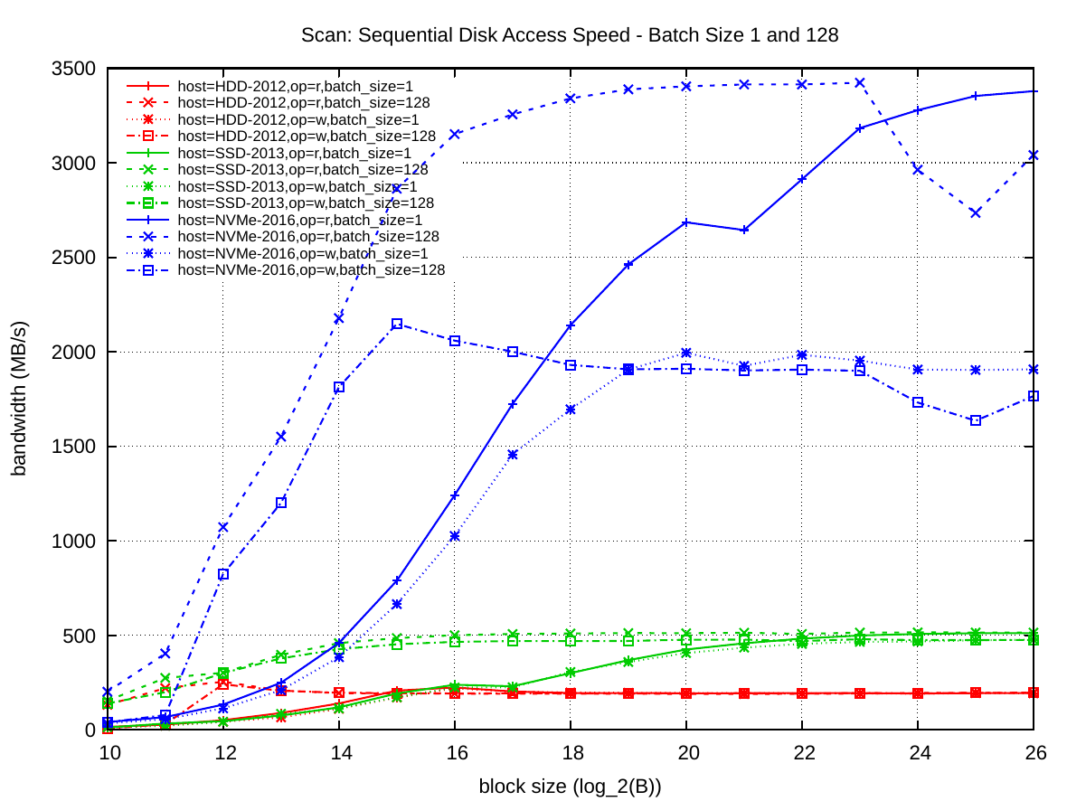
Here is batch size one. Follow the blue lines for nvme. Scan is sequential. Random is random. Both read and write is listed here. Sequential read is the further ahead.
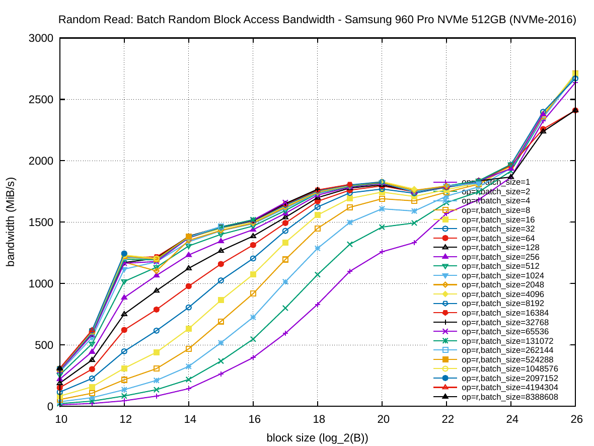
Final graph on the matter:
Last edited:
D
Deleted member 11852
Guest
Remember what Mark Cerny said about the I/O and the software stack. Then go check some of the Linus Tech Tips videos on super fast storage solutions and their benchmarks in Windows and Linux. Then think AGAIN about what Mark Cerny said about I/O and the software stack.I'm just trying to figure out how NVMe sequential reads and random reads are nearly the same in terms of data transfer. Which I think you're telling me it is, provided the OS and file-system has no issue doing it. But if these specs remove OS and filesystem from the equation, it would appear these numbers aren't the same.
But how is that going to affect specs outside of that? I posted some stuff from a blog. It's up above. There is nothing there that indicates random and sequential is the same speed.Remember what Mark Cerny said about the I/O and the software stack. Then go check some of the Linus Tech Tips videos on super fast storage solutions and their benchmarks in Windows and Linux. Then think AGAIN about what Mark Cerny said about I/O and the software stack.
D
Deleted member 11852
Guest
But you already said you didn’t know what the numbers represent. You can’t infer the information you are trying to understand without more information. When different metrics are used (Mb/s and IOPS) without explanation, query that. They’re your numbers not mime!But how is that going to affect specs outside of that? I posted some stuff from a blog. It's up above. There is nothing there that indicates random and sequential is the same speed.

Okay so I think I know where you guys are going.But you already said you didn’t know what the numbers represent. You can’t infer the information you are trying to understand without more information. When different metrics are used (Mb/s and IOPS) without explanation, query that. They’re your numbers not mime!
I cleared up my post above with the graphs
If you compare
Sequential Read ^12 block size, 128 Batch size
It's about 1100MB/s
If you do random Read ^12 block size, 128 batch size
It's about 750MB/s
If you do 8Mi batch size for random read at ^12, it's nearly the equivalent of sequential read at 128 batch size, I think even a little higher than sequential.
Which is super respectable and amazing!. This is the 4KiB block size you guys are referring to. But the problem is that 4KiB block size is no where close to the maximum throughput of this SSD.
At the higher end random reads can't compete.
My issue here is how these drives are going to be obtaining 3500+ MB/s with such a small block size, when it's clear say for this drive, you're going to need larger block sizes to obtain those higher bandwidth numbers.
Unless something is missing from my understanding here.
as for OS.
These two parameters are vital when designing and implementing external memory algorithms. The experiment was designed to see how these parameters change with the underlying storage architecture. The batched I/O requests are submitted by FOXXLL/STXXL to the Linux kernel using the asynchronous I/O aio interface. While preparing these experiments, I optimized FOXXLL's I/O queues to submit batches to the linux kernel instead of individual requests (see commit foxxll@c400389). This patch improved throughput on the fast NVMe by about 6% for random I/O.
All experiments were run with transfer block size B ranging from 1 KiB to 64 MiB. According to their specifications sheets, all tested devices internally have 4 KiB sectors. The batch size was varied from 1, where only a single request in issued to the device at once, up to 128 for the Scan experiment and up to 8 Mi for Random.
The full result set is available as a gnuplot PDF , the benchmark programs are part of the STXXL/FOXXLL library, and the raw result data (278 KiB) can be downloaded as a zip file.
Last edited:
Okay so I think I know where you guys are going.
I cleared up my post above with the graphs
If you compare
Sequential Read ^12 block size, 128 Batch size
It's about 1100MB/s
If you do random Read ^12 block size, 128 batch size
It's about 750MB/s
If you do 8Mi batch size for random read, it's nearly the equivalent of sequential read at 128 batch size.
Which is super respectable. This is the 4KiB block size you guys are referring to. But it's no where close to the maximum throughput of this SSD.
At the higher end random reads can't compete.
My issue here is how these drives are going to be obtaining 3500+ MB/s with such a small block size, when it's clear say for this drive, you're going to need larger block sizes to obtain those higher bandwidth numbers.
Unless something is missing from my understanding here.
as for OS.
Developer still needs to package data to some kind of bundles and read it in larger chunks. i.e. there still is work to be done on how to organize and package data. Randomly trying to read 4kB blocks is not winning strategy unless ssd is replaced with something like optane. Similarly the kraken/zlib/... compression requires larger chunks to achieve good compression ratios.
ps5 has unusually many channels potentially helping on small random reads. 12 nand chips/channels to use for parallel accesses to small files. Assuming those files are conveniently located in different chips.
Indeed.Developer still needs to package data to some kind of bundles and read it in larger chunks. i.e. there still is work to be done on how to organize and package data. Randomly trying to read 4kB blocks is not winning strategy unless ssd is replaced with something like optane. Similarly the kraken/zlib/... compression requires larger chunks to achieve good compression ratios.
ps5 has unusually many channels potentially helping on small random reads. 12 nand chips/channels to use for parallel accesses to small files. Assuming those files are conveniently located in different chips.
We don't have the graphs for PS5. But I mean, they can't be maxing out their full SSD potential on 4KiB, that means iit's basically a flat line across all block sizes.
As per the blog; what he was trying to measure:
There are two main questions behind the benchmarks:
- what is a good block size B to achieve high throughput, and
- how many I/O requests k of blocks B have to be batched to fully utilize the storage devices (batch size)
So having more is channels is definitely going to help - but the characteristics of increasing bandwidth are still in favour of block size if I understand correctly.
If I have understood it correctly nand chips consist of blocks. Row in a block is page. Only small amount of blocks can be active at the same time. Only pages from active blocks can be read. Page could be for example 4k and the block could be hundreds of kB to few MB. When doing a random read we would first find the right block, prime the block and then read the page. There is finite number of blocks we can keep active. If block from which we want to read a page is not active the read is going to be "slow".
Part of the random test being so slow is hitting random blocks and having to prime the block before being able to read a page. If we could do even simple reordering of reads so it becomes more likely for read to hit already active block that would be nice perf win. One would assume a test for random reads would try to create load that would try to hit random blocks in a way that is most challenging for the drive.
If one thought random access to small pages is most important thing then the nand could be designed to favor small random accesses. Or one could just go with optane.
Yes, it's similar to banks for dram. The exact order is:If I have understood it correctly nand chips consist of blocks. Row in a block is page. Only small amount of blocks can be active at the same time. Only pages from active blocks can be read. Page could be for example 4k and the block could be hundreds of kB to few MB. When doing a random read we would first find the right block, prime the block and then read the page. There is finite number of blocks we can keep active. If block from which we want to read a page is not active the read is going to be "slow".
Part of the random test being so slow is hitting random blocks and having to prime the block before being able to read a page. If we could do even simple reordering of reads so it becomes more likely for read to hit already active block that would be nice perf win. One would assume a test for random reads would try to create load that would try to hit random blocks in a way that is most challenging for the drive.
If one thought random access to small pages is most important thing then the nand could be designed to favor small random accesses. Or one could just go with optane.
Many channels per chip (everything scales per channel)
Many panes per channel (this is random read iops)
Many blocks per pane (this is the erasure size, so impacts writes the most)
Many pages per block (this is the minimum read size per pane)
The smallest concurrent pieces are the panes. Each pane can have a request happening at the same time (caveats, it depends on the architecture of the chip). Multiply everything together by the average latency required to serve a request, and it gives the total iops. It only works if all panes can have a successive request in the command buffer on time.
The channel interface is always 8bit. So a single 1200MT channel is 1.2GB/s, but in practice only a fraction of it is the effective bandwidth, there's an overhead with error correction, commands, timings, polling, etc... And 1200MT is the top speed available. If that speed was the only important value, the PS5 12ch would be 14GB/s. So 5.5GB/s is slower inexpensive chips and the final figure includes all reasonable overheads.
Each channel gets a request ready for each pane, change page and block on each, read it to the page register, and transmit it on the channel while starting immediately with the next request in the queue during the transfer because there's two page registers per pane.
The physical limit is the number of request per pane, per channel, per chip, up to the limit of the interface of the channel.
Nand chips have 2 panes per channel, and we are starting to see 4 panes to double the iops. Future versions of nand might double this to 8 panes. We need more width because the latency is not improving much.
Random read latency is about 20 microseconds average, but this depends on the chip, it goes worse with TLC, QLC, and also improves as some vendor launches a better architecture, so it's always moving.
Hypothetical 12ch controller:
1/20us = 50000 completed transaction per second per pane
50k * 2 panes * 12 channels = 1.2M iops
That's the absolute hardware limitation. The rest of the steps are every single layer of the pipeline outlined on the Cerny presentation at GDC. There's a lot of step that can go wrong, and it looks like all of these steps are taken care by the i/o processor at full bandwidth until the data is in memory directly usable by the GPU.
Aren't these last two inverted? Many panes per block and many blocks per page.Yes, it's similar to banks for dram. The exact order is:
Many channels per chip (everything scales per channel)
Many panes per channel (this is random read iops)
Many blocks per pane (this is the erasure size, so impacts writes the most)
Many pages per block (this is the minimum read size per pane)
Yes, it's similar to banks for dram. The exact order is:
Many channels per chip (everything scales per channel)
Many panes per channel (this is random read iops)
Many blocks per pane (this is the erasure size, so impacts writes the most)
Many pages per block (this is the minimum read size per pane)
The smallest concurrent pieces are the panes. Each pane can have a request happening at the same time (caveats, it depends on the architecture of the chip). Multiply everything together by the average latency required to serve a request, and it gives the total iops. It only works if all panes can have a successive request in the command buffer on time.
The channel interface is always 8bit. So a single 1200MT channel is 1.2GB/s, but in practice only a fraction of it is the effective bandwidth, there's an overhead with error correction, commands, timings, polling, etc... And 1200MT is the top speed available. If that speed was the only important value, the PS5 12ch would be 14GB/s. So 5.5GB/s is slower inexpensive chips and the final figure includes all reasonable overheads.
Each channel gets a request ready for each pane, change page and block on each, read it to the page register, and transmit it on the channel while starting immediately with the next request in the queue during the transfer because there's two page registers per pane.
The physical limit is the number of request per pane, per channel, per chip, up to the limit of the interface of the channel.
Nand chips have 2 panes per channel, and we are starting to see 4 panes to double the iops. Future versions of nand might double this to 8 panes. We need more width because the latency is not improving much.
Random read latency is about 20 microseconds average, but this depends on the chip, it goes worse with TLC, QLC, and also improves as some vendor launches a better architecture, so it's always moving.
Hypothetical 12ch controller:
1/20us = 50000 completed transaction per second per pane
50k * 2 panes * 12 channels = 1.2M iops
That's the absolute hardware limitation. The rest of the steps are every single layer of the pipeline outlined on the Cerny presentation at GDC. There's a lot of step that can go wrong, and it looks like all of these steps are taken care by the i/o processor at full bandwidth until the data is in memory directly usable by the GPU.
I wholeheartedly agree. The 5.5 GB/s throughput must refer to random reads. Why? Cerny specifically mentioned how the PS5 can cycle through its entire 16GB of RAM in 2s. Unless there is a groundbreaking file indexing system that Cerny somehow did not share, then the quoted figure is definitely random read speed. How is it achieved? I guess the customised I/O stack removes the overheads plaguing a more classic CPU controlled I/O system.
I don't think any of the numbers are that exact. 5.5 GB/s is going to be the drive's peak performance, because that's what we talk about. IO overhead might reduce that a bit, but then compression increases total data fetching into RAM. And lastly, we don't even populate the whole 16 GB with loaded data. A few GBs is reserved for the OS, and a bunch of GBs will be for run-time generated data. Best case, you'll populate about 13 GB of data with a restore of a memory dump. Cerny' numbers are going to more, "we can load about 16 GBs of data in about 2 seconds."  And the message is really, "we can get a game going in a few seconds," rather then, "here are the detailed benchmarks of our drive."
It's because nothing is ever that exact (like attainable VRAM bandwidth versus what we actually get to use) that we have to use peak paper specs to understand architectures/components, and then we can be caught out by strange exceptions dramatically decreasing the peak number.
It's because nothing is ever that exact (like attainable VRAM bandwidth versus what we actually get to use) that we have to use peak paper specs to understand architectures/components, and then we can be caught out by strange exceptions dramatically decreasing the peak number.
Any game developer would be giant idiot if best they can do is random reads. Or it's a very unusual game that has nothing functioning in predictable way. That would be one frustrating game to play.
For sake of completeness random reads on optane look like diagram below. I think this illustrates pretty well the weak point of standard ssd
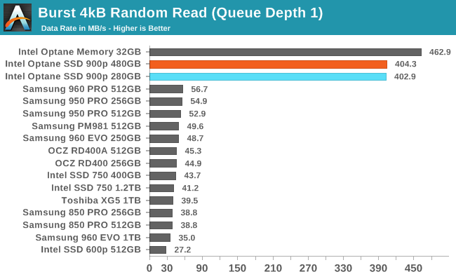
https://www.anandtech.com/show/12136/the-intel-optane-ssd-900p-480gb-review/5
For sake of completeness random reads on optane look like diagram below. I think this illustrates pretty well the weak point of standard ssd

https://www.anandtech.com/show/12136/the-intel-optane-ssd-900p-480gb-review/5
I had to look it upAren't these last two inverted? Many panes per block and many blocks per page.
They're called planes not panes (oups), and there's one more level with many planes per die, many dies per channel. So the parallelism is related to dies count without limitations, or planes count with some limitations. The page registers are per die not per plane.
I finally found a recent source, instead of going by really old stuff:
https://www.snia.org/sites/default/..._Second_Latencies_in_NVMe_Enterprise_SSDs.pdf

This is showing what we can expect from a modern pcie 4.0 nvme:
8KB pages
4 planes per die (so the full register is 32KB)
50us latency
6.5GB/s seq
1.7M iops at 4KB
So that would saturate 6.5GB/s with 4KB reads, but it needs a lot of dies per chip. It depends how "dies" are calculated.
This one is old and doesn't apply as much to modern chips, but it explains the complexity of spreading the requests to maximize parallelism internally:
https://www.usenix.org/system/files/conference/hotstorage12/hotstorage12-final55.pdf
Prediction: Sony will have a fixed 32KB access size, because they have only 512Gb per channel which limit the number of dies per ch.
Any game developer would be giant idiot if best they can do is random reads. Or it's a very unusual game that has nothing functioning in predictable way. That would be one frustrating game to play.
For sake of completeness random reads on optane look like diagram below. I think this illustrates pretty well the weak point of standard ssd

https://www.anandtech.com/show/12136/the-intel-optane-ssd-900p-480gb-review/5
Wow optane is a giant leap over the already beastly 960 in those operations. Too bad its so expensive still but i definitely want one
non random reads it's not the best however.Wow optane is a giant leap over the already beastly 960 in those operations. Too bad its so expensive still but i definitely want one
In a OS based experience, optane is ideal.
In a tightly packaged environment like games, I think going with sequential read as the main performer is ideal.
Any game developer would be giant idiot if best they can do is random reads. Or it's a very unusual game that has nothing functioning in predictable way. That would be one frustrating game to play.
For sake of completeness random reads on optane look like diagram below. I think this illustrates pretty well the weak point of standard ssd

https://www.anandtech.com/show/12136/the-intel-optane-ssd-900p-480gb-review/5
Mark Cerny explained it or read the patent. Random reads aren't a problem if you don't use 4k files. Out of menus, there is not 4k files in current-gen games. And same read Sony patent all files from 64 kb and above have no speed problem on Sony SSD. And Sony advise to merge 4k files if you need to read many at the same moment. For example, merge elements of the menu of the same screen inside a unique file, transform it in RAM.
From jayco measurement on Doom Eternal and Wolfenstein: The New Order
https://forum.beyond3d.com/posts/2117126/

4K files aren't interesting for games because out of save files and menus they aren't inside gameplay assets of modern games.
jayco said:I think I got more 256K and 512K readings in Doom Eternal because in Wolfenstein the tool crashed in the middle of the game play, so it only recorded the HDD activity while playing but not when loading the save file and the game itself.
https://www.resetera.com/threads/ps...nd-sonys-ssd-customisations-technical.118587/
Sony patent said:If a file size is small such as 4 KiB or so, it is necessary to complete processing within 0.4 μseconds per file so as to provide a 10 GB/second transfer rate. If read requests in such small units are issued frequently, parallelization effects will be marginal. Besides, the transfer rate of the main CPU 30 is more likely affected by the transfer rates of the sub-CPU 32, the flash controller 18, and the flash memory 20, easily increasing latency and resulting in a lower transfer rate of the main CPU 30. Therefore, if a data access request in such a small size occurs every millisecond or so, a plurality of files are combined into a single file and a data access request is issued in units of 10 MiB or so, thus providing a 10 GB/second transfer rate with high robustness.
- Status
- Not open for further replies.
Similar threads
- Replies
- 805
- Views
- 87K
- Locked
- Replies
- 3K
- Views
- 311K
- Replies
- 37
- Views
- 3K
- Replies
- 22
- Views
- 9K
